We is used to suggest a small integrated amplifier or the power amplifier with tone control circuit Were combined on the same PCB are 20watt Integrated Amplifier by TDA2005, but them is Mono.
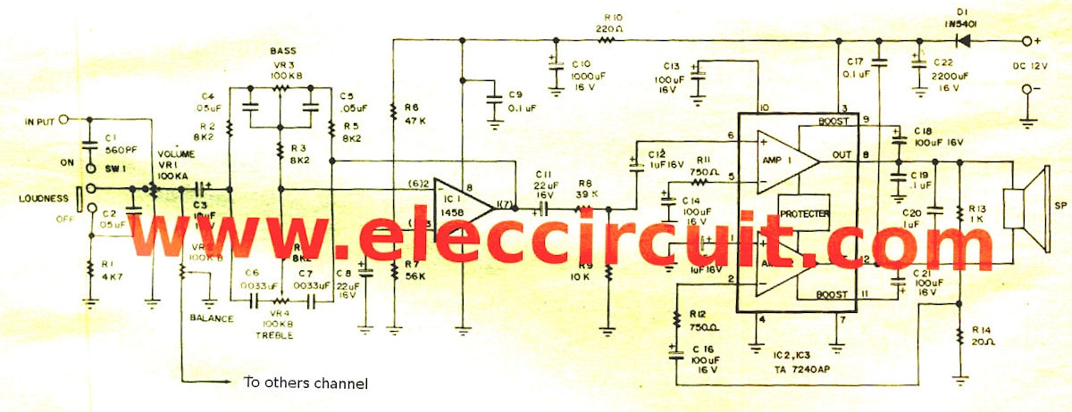
Today we see the 19W stereo integrated amplifier IC-TA7240AP, ideal for small rooms Or use the car because the power supply only 12 volts.
And the compact, buttons are placed on the PCB., To increase a convenient way to build. No wiring, you just have to connect speakers, Enter the signals Ready to listen immediately.
Special feature
-Power amplifier types : bridge amplifiers
-Output Power : 19 watts/channel at load 4 ohms 12volts.
-Wide supply voltage range: 9V to 18V.
-Supply current: over 1.5 amperes
– Total Harmonic Distortion Noise(THD): 1% at 15 watts and 10% at 19 watts
-Noise signal : lower than 0.14 mV
-The protection system : Thermal shutdown, over high voltage and short output.
-Boost up rate of tone control : + 20dB
The working principle of circuit
In figure 1 Because of the two-channel circuit same, therefore, draw only one channel. The numbers in the parentheses of IC1, is pin position in the circuit,other one channel.

Figure 1 the 19W Stereo amplifier circuit using TA7240AP
The working of circuit are separated as 2 sector :
A firstly is IC1 as a tone control circuit and second sector is IC2 as the power amplifier.
In the tone control circuit, a signal flow to input through volume-VR1, which is adjuster a sound level as you need.
They are C1, C2, SW1 and R1 as a loudness circuit, to boost up level sound to high and low frequencies.
While open low sound,if VR1 is turned up about halfway, the loudness circuit will do not works. When signal through VR1 and VR2 that adjusted level sound between left and right channel to balance are : the loudness button.
The other way will be fed to the tone control circuit to adjust bass-treble sound level by: VR3 is adjusted as bass button and VR4 is adjusted as treble button.
The boost cut rate of circuit is approximately + 20dB then this signal will be entered to pin 2 through IC1 amplify to pin 1.
The some signal will be fed back to R5 and C7 to control level of the bass-treble sound.
The R6, R7 and C8 act as a reference voltage in to pin 3 of IC1 to the op-amp IC1 use with positive and negative voltage.
Which normally IC1 always required the positive, negative and ground power supply.
The signal is adjusted output pin 1 of IC1 through C11,act as the coupling signal in to the power amplifier sector. By in to C12, R8 and R9 are used to set amplitude of signal from the tone control sector that proper feed to the power amplifier sector.
IC2 is the amplifier section, internally consists of two in one amplifier , each set will have power output of 5.8 watts per channel, then when we take them to bridge together so cause higher power up into 19 watts per channel.
Since we set this both amplifier that 180-degree phase difference the output to directly speaker. So signal is boost up signal rise.
– C13 is filter to protects internal IC voltage or the Ripple Filter.
– The C14, R11 And C16, R12 are the negative feedback.
– C18 and C21 act as boost tap to add amplify gain of IC1 rise.
– C17, C19 and C20 acts as protection oscillate in high frequency.
– R13 and R14 are determined the gain of IC1.
– C10, C22,R10 are filter of the power supply to smooth.
You may also like these:
The building and applications

Both the power amplifier circuit and the tone control circuit in same PCB, so very easy to build. Unnecessary wiring Avoid the extra time to create.
Figure 2 Actual-size,Single-sided PCB layout.
Figure 3 The components layout of this circuit.
You can solder as the levels of the parts on components layout as Figure 3 only full correctly
Cautions to build are a position the IC pin, the polarity of the diode, electrolytic capacitors. Since this circuit use quite a lot of the electrolytic capacitors, So be careful about the polarity is correct.
When put all components fully,then must attached the heat sink with TA7240-IC and to connect a ground to all potentiometer to protects all noise.
Then later, connects the left and right signal to input and insert the power supply to the circuit, Ready to listen to your favorite music now.
Learn How to use LM386 audio amplifier
The components list
Resistors ¼ watts 5%
R1: 4.7K
R2-R5: 8.2K
R6: 47K
R7: 56K
R8: 39K
R9: 10K
R10: 220 ohm
R11, R12: 750 ohms
R13: 1K
R14: 20 ohm
Capacitors
C1: 560pF ceramic
C2, C4, C5: 0.05uF 50V, Mylar
C3: 10uF 16V, Electrolytic
C6, C7: 0.0033uF 50V, Mylar
C8, C11: 22uF 16V: Electrolytic
C9, C17, C19, C20: 0.1uF 50V___Mylar
C10: 1,000uF 16V: Electrolytic
C12, C15: 1uF 16V, Electrolytic
C13, C14, C16, C18, C21: 100uF 16V, Electrolytic
C22: 2,200uF 16V, Electrolytic
Potentiometer
VR1: Volume 100K (A)___Dual unit with center tap.
VR2: Volume 100K (B)__Single unit
VR3, VR4: Volume 100K (B)__Dual unit
Semiconductor
IC1: LM1458, NE5532, LF353, TL072 the either number.
IC2, IC3: TA7240AP
D1: 1N5401, 3A 50V Diode
Others.
– PCB
– Socket IC-8 pin
– Heat sink.
– toggle switch 6 lead.
Related Posts


I love electronics. I have been learning about them through creating simple electronic circuits or small projects. And now I am also having my children do the same. Nevertheless, I hope you found the experiences we shared on this site useful and fulfilling.