From our last article on this subject, we learned that a transistor can function exceptionally well in an amplifier circuit. Therefore, today we are going to learn how to put this knowledge to use by designing a small signal amplifier circuit using transistors.
Suppose we have a small sound wave generator generating a signal with a peak-to-peak amplitude of around 30mVp-p (0.03Vp-p). If we were to feed it to a regular sound amplifier, most would not output anything, or some would just output an inaudible sound.
For it to work, we would need to increase this signal to around 500mVp-p first. The most common way is to use a preliminary signal amplifier circuit, commonly referred to as a preamplifier circuit.
It is often found in an audio system and used to amplify a weak AC signal.
Designing a small signal amplifier circuit
The design process in this article uses very few principles so that it remains easy to understand throughout.
From my experience, using this method nets us below a 20% error rate in a calculation, which is acceptable in most electronic circuits.
The required gain of the circuit
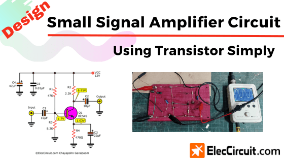
We would need a small signal amplifier circuit (preamplifier) that is capable of amplifying a voltage level of 30mVp-p to 500mVp-p, which amounts to around 16.7 times amplification (500mVp-p/30mVp-p). Also, its current needs to stay within the 10mA range because the input of most of the common main amplifiers only needs a very low current.
But given the fact that the minimum gain (hFE) of most small transistors is already 100 times, a single one of these transistors with an IC of around 100mA will be more than enough.
Choosing the transistor
We could use most small NPN transistors with a gain (hFE) of 100 and an IC of 0.1A or more. Such as BC549, S9013, 2N3904, or 2SC1815; the difference between them being the pinout.
Buy these small transistors at Amazon.com here (affiliated link)
But for today, we will use a BC549 because we do have many of these transistors lying around. It has around 200 gain (hFE) and an IC of 0.1A, which is enough for our usage.
Recommended:
- Experiment with transistor as switch
- Experiment with adjustable transistor circuits partially on-off
- Experiment with Parallel Transistors for More Current
Common emitter amplifier circuits
The most common form of a high-gain transistor circuit is a common emitter. Whereby its main operating principle consists of the Base functions as an input and the Collector as an output, whereas the Emitter connects directly to the GND.
As we might have known, transistors require a bias to function. There are generally three ways to bias a transistor, depending on how we set up the base bias, which includes:
- Fixed Bias
- Self-feedback Bias
- Voltage-divider Bias
Fixed Bias
It is the most basic out of all base biases. Hence, the collector voltage depends solely on the gain of the transistor itself. Which is not suitable for our usage here, thus we should look for other ways.
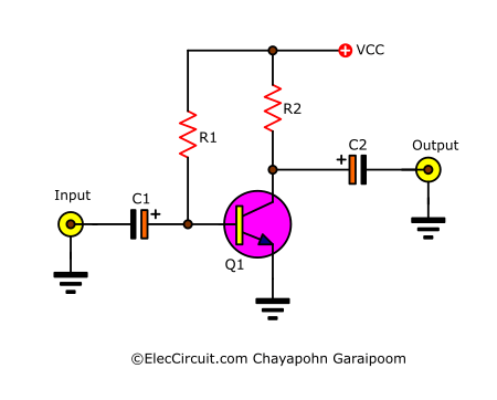
Self-feedback Bias
From the fixed base bias above, we move one end of the R1 from a positive power supply to receive a bias current from the collector of the transistor instead. In this configuration, it is referred to as a feedback base bias, as the transistor receives negative feedback through R1 (feedback resistor).
Now the collector voltage will not increase based on the gain of the transistor. Because when the collector voltage decreases, it will cause the base bias current feeding back to the transistor to decrease as well, ramping down the transistor, thus increasing the collector voltage, and vice versa.
This will counter any change in collector voltage, greatly improving the stability, which is why we often choose this type of circuit.
Making the circuit fall into class A
We want this small signal amplifier circuit to function well, with low distortion and a good frequency response. So, we will set this circuit to be a class A amplifier, but it will consume a lot of energy as the transistor works all the time.
Though not much of a problem for us because this signal amplifier circuit only requires a small amount of current, no higher than 5mA.
Class A amplifier circuits need the collector voltage to be around half that of the power supply. So that the transistor can amplify both the positive and negative parts of the waveform.
We also add another resistor (R3) at the emitter to protect the transistor against high base current and limit the current properly so that we can set the voltage at any particular point more easily.
Determining the bias current and voltage
In these types of circuits, there are both DC and AC at play. It starts with a DC bias, and the transistor circuit works in the form of class A.
Then, the AC signal flows into the circuit through capacitor C1 to be amplified by the transistor circuit; the higher AC signal will then flow through capacitor C2 to the output.
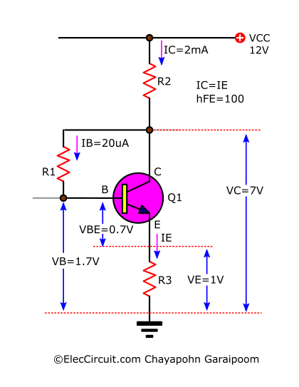
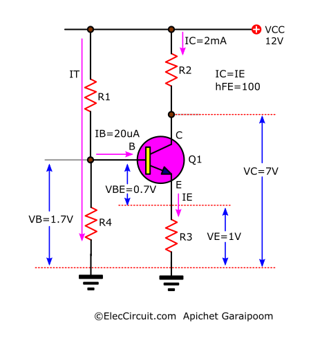
When finding the value of the components, we first cut the capacitors out of the picture and then set the voltage and current of each point in the circuit, as shown in the illustration below.
What we know:
- VCC (the power supply’s voltage) is 12V.
- The transistor requires at least 0.7V of VBE (base bias voltage) to function.
- The transistor’s hFE is 100, and its IC is 0.1A by default.
- IC is equal to IE (IC is the current that flows through R2 or IR2, whereas IE is the current that flows through R3 or IR3. Which is identical, so we can infer that IC = IE, implying that IR2 = IR3.)
What we determine:
- -VC is 7V; we set the collector voltage (VC) at around half that of the power supply (we round it up to 7V as it’s easier to calculate later on).
- VE is 1V; we set it to this value because it gave the transistor a wide voltage range between its C and E.
- VB is 1.7V; it is a combination of VBE and VE, which are 0.7V and 1V, respectively.
- IC is 2mA; which is sufficient for the transistor itself and its output; it is also low enough that it would not heat up much despite being a class A amplifier.
Starts calculating
Our objective is to find the values of R1, R2, and R3.
We will start from the easiest to the hardest.
(1.) R3 = VR3÷IR3
VR3 = VE = 1V
IR3 = IC = 2mA
Substituting equation (1)
R3 = 1V÷2mA = 0.5kΩ
But there is no resistor of this value, so we chose R3: 470 ohms instead.
(2.) R2 = VR2÷IR2
VR2 = VCC – VC
VR2 = 12V – 7V = 5V
IR2 = IC = 2mA
Substituting equation (2)
R2 = 5V÷2mA
R2 = 2.5kΩ
We will be using 2.2kΩ for R2 instead.
(3.) R1 = VR1÷IR1
VR1 = VC – VB
VR1 = 7V – 1.7V = 5.3V
IR1 = IB
IB = IC ÷ hFE
= 2mA÷100
= 20µA
Substituting the equation R1 = 5.3V÷20µA gives us 0.265MΩ, of which none are built, so we will use R1: 270kΩ instead.
About capacitors with AC signal
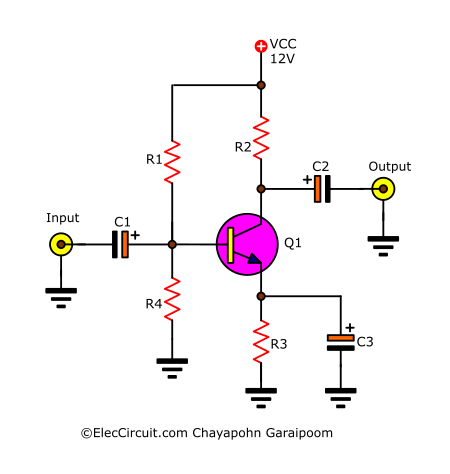
First, we put the capacitors that we have set aside back into the circuit, as shown below.
The original capacitors (C1 and C2)
I am quite hesitant about telling my daughter the process of calculating the values of C1 and C2. Because it is quite complicated, as they operate in an AC, which has more variables than in a DC.
Read also:
- Uses of capacitors | Capacitance | RC circuit time constant
- What is capacitor? Principle working, types and how it works
In this article, we use a try-out and experiment method to find the capacitors’ values. But in the future, when we actually have fundamental knowledge, we may learn in-depth about this subject.
Like watering a plant, we should not overwater it when it is still a sapling, but we should start small and then gradually increase the amount of water as it grows.
We tested by playing through a sound frequency with a range of 20Hz to 20KHz and switches between capacitors of each value.
The result we got is that the sound differences are unnoticeable at a capacitance ranging from 1µF to 22µF. We, thereby, choose a 10µF 50V as there are many of them in stock.
The C3 capacitor
The C3 is a coupling capacitor, which increases the gain in an AC signal. As if the C3 is a very low-resistance resistor, increasing the gain of the transistor thereof.
We tried using capacitors in a capacitance range of 4.7µF to 47µF, which gave us the same result, so we chose 22µF.
Noise killer
C4 helps increase the efficiency when there are load spikes. C5 is a bypassing capacitor preventing noise from interrupting the circuit.
Usually, these noises have a very high frequency, and when it sees C5, it will think that C5 is a very low-resistance resistor, thus flowing through it to the GND.
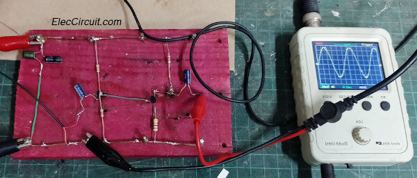
Testing the circuit
Then, we test the circuit by measuring the voltage at each point. The voltage reading is almost the same as what we have determined, which is VC = 6.27V, VE = 1.24V, and VB = 1.86V.
Next, we try inputting a 30mVp-p 1KHz sine wave signal into the circuit, outputting around 2,500mVp-p or a gain of about 83.3, which is enough for our needs.
See an example circuit using this method:
- Simple Condenser Mic Preamplifier Circuit using 2N3904
- Cheap & Small hearing aids circuit project
- The medium Impedance Preamplifier circuit
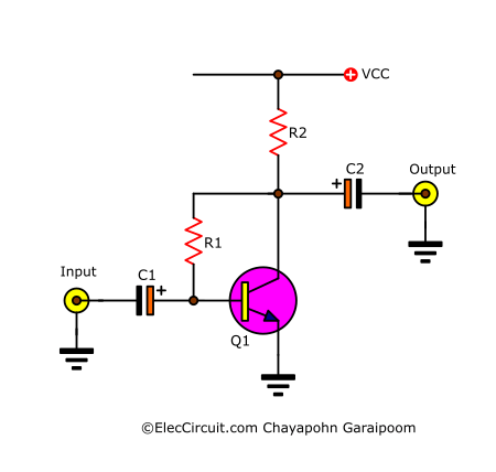
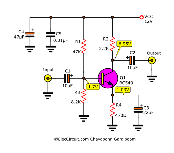
Voltage-divider bias
Another way that I would like to introduce you to is a voltage-divider bias, with the addition of a resistor (R4) being the only addition we made to the self-feedback bias.
A voltage-divider bias, or what may also be known as a bridge bias, gives out a very stable collector voltage with regard to any kind of transistor.
Determining the bias current and voltage
As before, we will classify it as a class A amplifier. As well as the process of finding the value of each component, that is, determining the current, voltage, and such.
Starts calculating
What we are looking for are the values of R1, R2, R3, and R4.
For the R2 and R3, it uses the same calculation as the self-feedback bias, so we will use that instead.
R2 = 2.2kΩ
R3 = 470Ω
The rest, we would have to find it ourselves.
Finding R4
We add another variable, IT, which is the current that flows through R1 and R4.
RT = R1 + R4
Which is equal to
(2.) RT = VCC ÷ IT
We set IT to be around 10 times the IB so that the base bias has greater efficiency.
And we know that IB = 20µA and VCC = 12V.
Thereby, IT = 10×IB = 10×20µA = 200µA.
Substituting the equation (2)
RT = 12V ÷ 200µA = 60,000Ω = 60kΩ
Using the same equation as in a voltage-divider circuit
We know that VC = (VCC × R4) ÷ RT.
Therefore
R4 = (VB × RT)÷ VCC
We also know that VB = 1.7V, RT = 60,000Ω, and VCC =12V.
Putting them in
R4 = (1.7V × 60,000) ÷ 12V
= 8,500Ω = 8.5kΩ
But there are not any bulit, so we use 8.2K for R4 instead.
Finding R1
R1 = RT – R4
R1 = 60kΩ – 8.5kΩ = 51.5kΩ
The closest of which is 47kΩ; we will be using that instead.
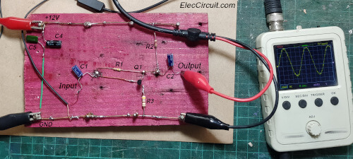
Testing this small signal amplifier circuit
As for the capacitors and other components, we will use the same as before.
Then we assemble the circuit, try inputting a voltage, and measure the voltage at different points. Which is almost the same as what we have calculated.
VC = 6.95V , VE = 1.03V, VB = 1.7V
Next, we apply an input, and as before, the resulting signal is excellent and also more stable.
Note: If you want a PCB design of this small signal amplifier circuit, do let us know, and we will create one.
Want more brilliant ideas? Here’s how to get them through electronic circuits.
Conclusion
We saw that creating a small signal amplifier circuit using a transistor in a class A configuration is not too complicated.
We might be able to modify things, such as components, power supplies, et cetera, to get a different result from this circuit.
In the future, we might try to create a small amplifier circuit that uses three transistors instead of one. Be sure to let us know if this ideal interests you in some way.
GET UPDATE VIA EMAIL
I always try to make Electronics Learning Easy.

I love electronics. I have been learning about them through creating simple electronic circuits or small projects. And now I am also having my children do the same. Nevertheless, I hope you found the experiences we shared on this site useful and fulfilling.

a materia merece um 10, altamente didatica, compreensiva, e muito gostosa de recordar, ja que tenho 3 faculdades de engenharia eletronica…mas esquecemos algumas teorias do passado.gostaria de receber terias sobre fontes chaveadas. formei a ultima em 1984 e essas fontes eram poucas exploradas, entao nao tive teoria aprofundada. no brasil nao se acha tecnico para conserto de fontes de pc justamente pela complexidade de funcionamento e peças dificeis de encontrar, parece que tem componentes que nao existem nos livros. diodos encapsulados..etc…obrigado por tudo
Hello,
With great pleasure. We are so glad that this article was helpful to you. If you have any other suggestions, We will be happy to improve, and we will share our experiences in electronics that we have learned ourselves. I hope you will continue to follow us. Thank you too.