Today we will be learning electronics through creating a simple circuit again. This time, it is the led blinking circuit as Bicycle Taillight. That will emit a flashing red light on the back of our bicycle to increase safety at night.
We have designed this circuit with basic electronic principles in mind, so there would not be an IC and it would use low power.
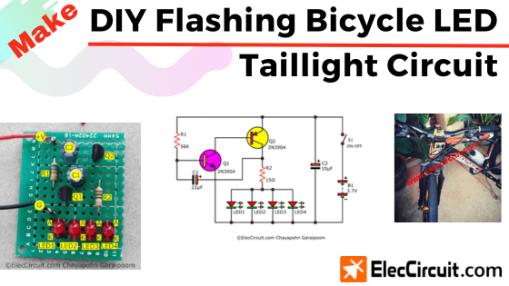
My son built this circuit about ten years ago. But now my daughter is remaking it again because it is easy to make and perfect for learning about basic transistor oscillator circuits.
Things we aim to achieve
- Using transistors instead of ICs because they are simple and economical.
- Using four 3mm red LEDs in parallel, as they only need 10mA of current each, combining up to just 40mA.
- Using a single 3.7V Li-ion battery. Though we have thought about using a 9V battery, as it has a small size and the downside of only supplying around 150mAh. Which would not last long enough with our light. So we switch to 3 Ni-MH batteries in series with a combined voltage of 3.6V, giving us 2,100mAh. Translated to more than 52 hours of use, with the downside of being too bulky.
Therefore, we figure that for today, we will use this 3.7V Li-ion battery that can supply 2000mAh of current in a compact size.
How this LED blinking circuit works
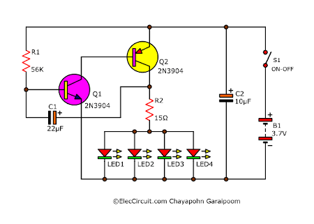
The circuit below is the led blinking circuit. It is quite simple because there are few components. But learning its working principles is very interesting.
Similar to a regular oscillator circuit, its order of operation starts with the transistor working and then stops through the feedback of a negative voltage from the capacitor discharging.
For the sake of understanding, let’s simplify this diagram further by substituting both transistors with a switch.
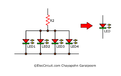
As well as the LED circuit, making it a single LED for now.
Understanding LED Blinking Circuit
With that idea in mind, let’s now look into the simplified diagram below.
When LED is on
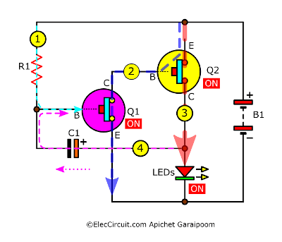
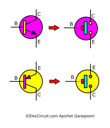
(1) First, the base current from B1 will flow through R1 to bias Q1, turning it on. (2) Now, between C and E of Q1, they are connected just like a closed switch. (3) Thus, completing the circuit allows the current to flow through E and B of Q2, turning it on as well.
Letting the current flow through and power the LED, (4) while at the same time charging the C1. It will remain in this state for a short moment until the C1 is fully charged.
When LED is off
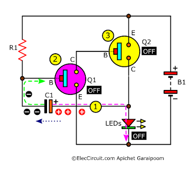
This phase started with C1 discharging a negative voltage, which flowed into B of Q1. So, the Q1 switches to a cut-off state, preventing current flow between C and E—it can also be thought of as an opened switch. Thus, no current will flow through E and B of Q2, turning it off in the process.
In turn, shut off the LED as well, but just for a short while. Because when C1 discharges completely, the current at B of Q1 will return to positive yet again through the base current from R1. This cycle will continue over and over again, causing the LED to flash repeatedly.
What does each component do?
C1 controls the frequency at which the LED flashes; if its capacitance is high, the LED will flash at a slower rate. But if the capacitance is too low, the LED will flash at a rate so high that it appears dim. From our experiment, C1 should be in the range of 10uF to 47uF.
R1 affects the base current flowing to Q1, and if it is higher than 220K, the brightness and flash rate of the LED will decrease.
R2 determines the brightness of the LED, as it controls the amount of current that the LED receives.
We can calculate the resistance of R2 easily by using this formula:
R2 = (Vbatt – VLED)/ILEDs
Vbatt = 3.7V
VLED = 1.8V
As we want all LEDs to be at full brightness, we set the current to around 20mA for each of them, amounting to about 80mA (0.08A).
ILEDs = 0.08A
Now we plug those values into the formula:
R2 = (3.7V-1.8V)/0.08A
R2 = 23 ohms
However, due to the LEDs flashing, their average current decreased. So we choose 15 ohms instead to compensate for the current losses.
Parts will you need
This circuit has an electronic components list that is quite small; you can find it anywhere.
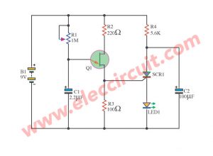
Q1: 2N3904, 40V 0.2A NPN Transistor
Q2: 2N3906, 40V 0.2A PNP Transistor
C1: 22µF 25V, Electrolytic Capacitors
C1: 10µF 25V, Electrolytic Capacitors
R1: 56K, 0.25W Resistors tolerance: 5%
R2: 15Ω, 0.25W Resistors tolerance: 5%
LED1-LED4: Red 3mm LEDs
3.7V battery, switch, and more
How to build
My children have built this circuit twice already, with each time having a different way of putting the circuit together.
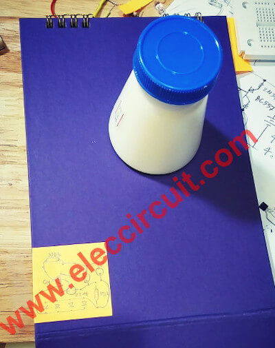
Assemble on cardboard
My son built it in this way about ten years ago. By taking cardboard from an unused tabletop calendar. And it has been working quite well, with the upside of not having to use a PCB.
Here is a short overview of how to build it.
We worked out the component layout on regular paper. Then stick it on the cardboard with glue.

Then, use a pointy small metal rod to poke a hole in the cardboard to put the components on.
Put each component according to the layout drawn.
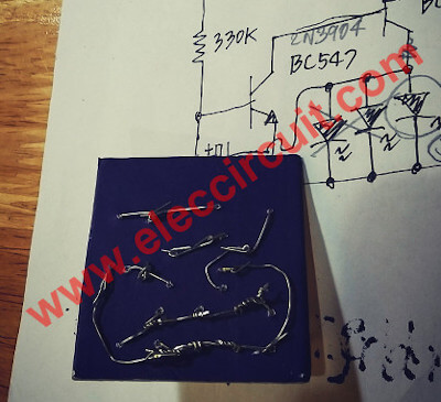
Bend a leg of a component and twist them together to create a joint as labeled on the other side. If the leg would not reach, then use small copper wires, sized around 24 AWG, to join them together.
Solder each of the connected joints.
Check each and every connection thoroughly.
Try applying power to the circuit; we will see the LED blinking rhythmically. If it is not to your liking, then change C1 or R1, as we have mentioned.
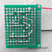
Anyhow, this way of assembling may not be suitable for a small circuit, and it also has a low resistance against humidity and is also ugly-looking.
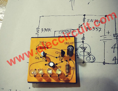
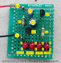
Assemble on perforated PCB
Recently, my daughter has also built this circuit, although now she has assembled it on a perforated PCB. Making it smaller and more rigid.
Conclusion
This flashing bicycle LED taillight circuit is easy to build, but it is still an interesting oscillator circuit. By just combining two different types of transistors, one resistor and one capacitor, we can generate frequency. In the future, we will learn more about it by experimenting with different components and values or even adapting it to other roles. It is quite an interesting circuit for its size.
Download This
All full-size images and PDFs of this post are in this Ebook below. Please support me. 🙂

I love electronics. I have been learning about them through creating simple electronic circuits or small projects. And now I am also having my children do the same. Nevertheless, I hope you found the experiences we shared on this site useful and fulfilling.

Awesome, Thanks.
Hi Salim Khan,
Thanks for your feedback.
My dream and vision is to invent a powerful electronic by hydropower
To anyone reading… I have a bunch of little electrical parts such as: transistors, diodes, led bulbs (white, red, and green). Jameco; Fairchild; lite -on; and so on. I really have no use for em and don’t know what they are really for. Everything is still new, never been used sealed in separate packages in quantities of 10pcs. If anyone interested in buying these from me please call me at 415 724 7358.
Great circuit in which I am planning on making, but before I do, I was wondering what is the wattage of the 15 ohm resistor in the circuit?
It looks like a 1/2 watt resistor, am I right?
Thanks for the help and your contributions to those in the community that share the same interest in electronics.
David
What represent R1 330K?
Hi Adrian,
You can use 100K to 390K resistor.
Hi David,
Thank you so much.
Yes, you can use 1/2W resistor.
Same components can for 12 v supply and 12 v beeper
R1 Is A Feedback Resistor For The Osccillator Circuit
OOPs!!!!! Oscillator Circuit
What is the Ohm of R1 in the Fast Blinking LED Bike Lighting Circuit? Can’t see it in the text
Hi Dieter,
Thanks you like this circuit.
We feel sorry, forget to put parts list.
Are those transistor must be identical ?
Hi,
It would be best to use different transistors, both NPN and PNP. However, the PNP transistor is the one that drives power to the load. So, you should use one that is large enough for the load.
You have an error on the schematic.
Both PNP and NPN transistors have same reference.
Correct the PNP
Hi,
It is correct we use both NPN (Q1) and PNP (Q2) transistors.
Thanks,