Today, let’s learn about the principles of Mobile or Cell Phone Charger circuits in a simple way for a beginner.
You might be reading this article on your web browser on your cell phone, right? Your phone is powered by a Li-on battery, and when it runs out of power, it has to be charged with a cell phone charger or mobile charger. But the Li-on battery should always be kept fully charged.
How it works
Nowadays, the cell phone charger converts AC mains to 5V stable voltage for charging the cell phone (built-in the cell phone there is already a charging system and Battery Management System).
Inside the cell or mobile phone charger is just a 5V switching power supply. It is both small and cheap.
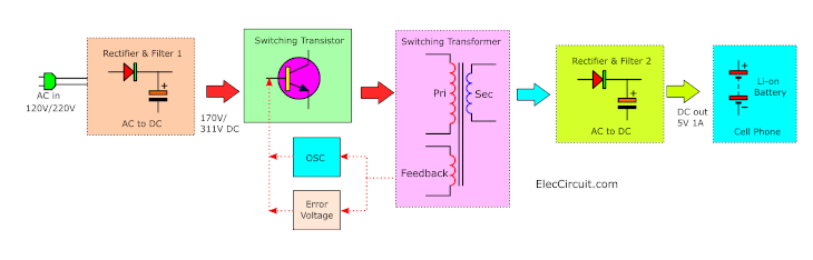
There are many 5V charger circuits out there. But we’ll start with a simple circuit first. Refer to the block diagram below to understand the broad concept.
At the first Rectifier & Filter block. It converts from a high-voltage AC main to a higher DC voltage. The input can be 110V AC to 240V AC.
For Example:
The North American system converts 120V AC to 170V DC. But the European system converts 220V to 311V DC.
This block contains a half-wave rectifier circuit.
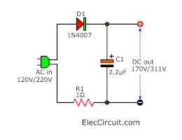
The AC main flows through a fuse resistor R1. It will break or self-destruct when there is too much electricity. Then D1 rectifies the AC (Alternating Current) to a pulsating DC (Direct Current). Then, it is filtered to a smooth DC voltage of 170V or 311V.
Meet the RCC Switching Power Supply
There are various switching power supply systems. It is well known that they have at least two main parts: an oscillator and a transformer.
But if we need the circuit to have low output capacity, simple, and cost-effective as possible. We may have two choices: a Forward converter and a Ringing-Choke Converter (RCC).
But we chose the RCC system for the following reasons:
1. It is most widely used as a switching power supply with a quite low output capacity of fewer than 100 watts.
2. Use self-oscillated oscillation, which, considering the low cost and small size, has a pretty high efficiency.
3. The small number of parts consists of one transistor, a switching transformer, resistors, capacitors, and some other parts.
4. Only a simple driver circuit is required.
5. Does not need a filtering choke.
The switching transformer
This circuit has an interesting component, a switching transformer. It is a transformer that operates at high frequencies. It is easy to tell it apart from other transformers because of its very small size.
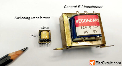
It serves to transform the AC voltage to a lower value, step-down transformer. This circuit uses T1 with 3 winding of coil:
1. Primary: A resistance of about 8.2Ω, about 200 turns of 39 AWG enameled copper wire.
2. Secondary: A resistance of about 0.2Ω, about 6 turns of 28 AWG enameled copper wire.
3. Feedback: A resistance of about 1Ω, about 10 to 20 turns of 36 to 39 AWG enameled copper wire.
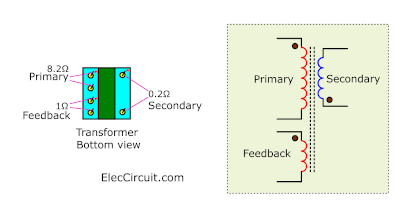
Note: AWG stands for American Wire Gauge.
If you cannot find a switching transformer of this size, you may pick one that is approximately 10-15 mm in size or similar. Each transformer may have a different winding resistance. But the important thing is that they have to have 3 coils, and the primary coil has the highest resistance of any other coil. May be 15–25 times greater than the secondary coil.
Switching transistor for Ringing-choke Converter
The transistor for RCC must have the essential characteristics of high hFE, high-speed switching, the ability to withstand high voltage, and a wide RBOA (Reverse Biased Safety Operating Area).
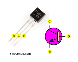
According to my experience, the MJE13001 transistor is commonly seen in a switching power supply because it is a high-voltage NPN BJT Transistor in TO-92 shape. And, for other basic features:
- hFE range (DC Current Gain): 5 to 40
- IC (Collector current): 200mA
- VCB Collector to base Voltage): 600V
- VCE (Collector to emitter voltage: 400v
- VEB (Emitter to base voltage): 7V
- TJ (junction temperature: 150°C
- Power dissipation at the transistor: 1000mW
- FT (Transition frequency): 8MHz
The basic operation of the RCC circuit
From the block diagram, we know that it used a switching transistor and a switching transformer. Next, we are going to learn how an oscillator (OSC) or flyback oscillator works.
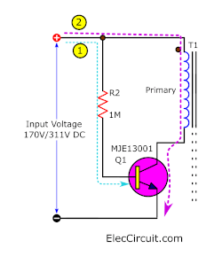
When the input voltage is applied. The base current (IB) flows through resistor R2. Biasing the transistor Q1, turning it on.
Secondly, the collector current (IC) flows through the primary winding and starts rising rapidly and linearly as shown in the graph, until it reaches the threshold level.
After a few moments, the feedback winding will start to increasingly release a low opposite (negative) voltage, charging the capacitor C3, and continuing to flow to the base of Q1. The VBE is negative voltage. It has greater power than the current flowing through R2. Consequently, the transistor turns off and the current stops flowing through the primary winding.
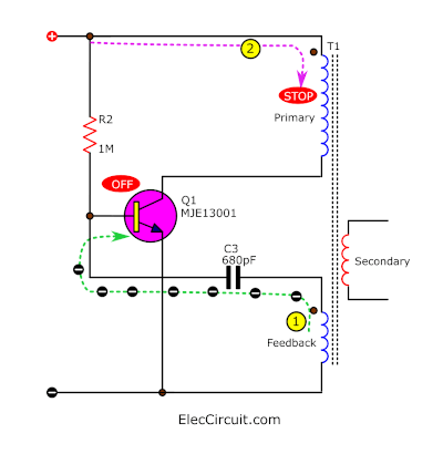
When the discharging negative current runs out. The base current starts to flow through R2 to bias the base of transistor Q1 again.
This cycle will continue forever at around 10,000 to 50,000 times per second. This frequency change depends on the input voltage and how heavy the load is.
See the Operation waveform of each part of the RCC system.
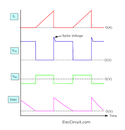
We can see the relationship between IC, VCE, and VBE as a transistor turns on and off.
And now we have an oscillator, or the flyback oscillator circuit.
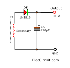
It also stores energy in the transformer during the period the transistor is on and outputs this energy to load through rectifier 2 when the transistor is turned off.
The rectifier & filter 2 is also the half-wave rectifier circuit, but now with a higher frequency. It is also better to use a Schottky rectifier diode, 1N5819, instead of the original 1N4007. Because 1N5819 is more efficient at higher frequencies.
And on the C5 filter capacitor, we swap out for a higher capacitance of 470µF to filter high current more smoothly.
Error Voltage Checker
How can we stabilize the voltage at 5V?
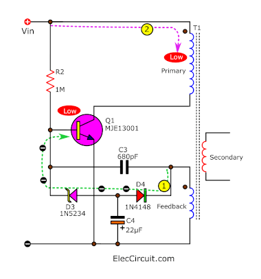
We add D4, C4, and D3 as the error voltage checker. Some AC voltage from the feedback winding flows to D4 and C4, half wave rectifier to a negative DC voltage. And, the D3 is a 6.2V Zener diode. is too high, and this negative voltage is also too high at more than 6.2V. The D3 is forward-biased, so some negative voltage pulls down the VBE of the transistor. Then, the collector current (IC) of the transistor is also lower. So, the output voltage eventually decreases.
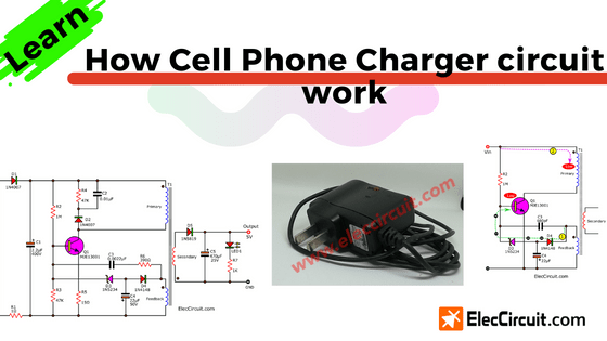
Finally, we take each part and assemble them into a complete Cell Phone Charger circuit.
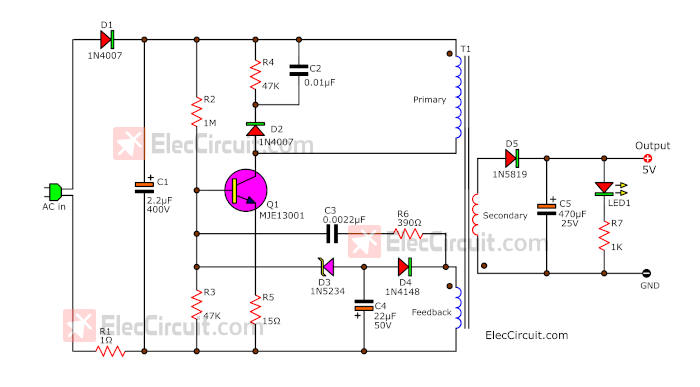
Due to the problem of spike voltage from the operation of the switching transformer (see above graph), It may cause damage to other components, especially the switching transistor. So, we put R4, C2, and D2. For the diode D2, it can absorb a negative spike voltage.
We also add R3 and R5 to improve the biased current of the transistor.
And, LED1 indicates the circuit is working, and R4 limits a safe current for LED1.
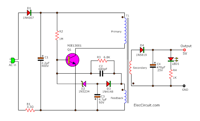
However, you may modify the new circuit to be smaller and easier. But there may be a problem with spiked voltage, so it is an option that you should consider.
Changing the output voltage
Choosing the voltage of the Zener diode
We may use the 1N5237 (8.2V 0.5W), which causes an output voltage of about 7.4V, for charging a 6V battery.
We will see that:
1. The output voltage of this adapter should be higher than the battery’s voltage by about 20%. If we use a 12V battery, the output voltage is about 14 volts.
2. The breakdown voltages (Vz) of the Zener diode should also be higher than the output voltage, around 20%.
Suppose the output voltage is about 14 volts. Therefore, we should use the 18 volts Zener diode.
The Zener diode in the circuit used 0.5 watts.
Good battery charger
While is charging, the battery is not hot. Thus, the life of a battery is a long time, and can recharge several times.
The disadvantage is it takes about 3 hours to charge because it is low current charging about 500mA to 800mA.
Read Also: Simple Li-ion Battery circuit with automatic cut-off
Conclusion
In the nature of this circuit, without a load, the output voltage is slightly higher. When the load is connected, the voltage can be reduced as needed.
The cell phone charger meets our needs: it is simple, small, and cheap, but it can also be made more efficient. Both have a better energy supply, maintaining a stable voltage.
Make Gel cell battery charger circuit
Sure, I want to see you grow up in electronics. Below is circuits list you may like it.
- 8 How to converter 12V to 6V Step down
- Power bank Mobile Charger Circuit using LM1086
- Many Simple 6V Power Supply Circuits
Download This
All full-size images and PDFs of this post are in this Ebook below. Please support me. 🙂
Related Posts


I love electronics. I have been learning about them through creating simple electronic circuits or small projects. And now I am also having my children do the same. Nevertheless, I hope you found the experiences we shared on this site useful and fulfilling.
hi sir,i’m verry happy with your site,coz i’m hobby electronic. Thank’s very much
With great pleasure I’m happy that like it, my dad teaches me every day, but it’s hard for me. But I’ll keep trying. 🙂
Thanks.
hallo,
die schaltung kann so nicht funktionieren. die verbindung von D3 und C3 darf nicht an den
emitter gehen. sie muss an die basis angeschlossen werden.
viele grüße
walter
Hi, this ckt is found to b very useful however it wud be better if u wud provide the details of the transformer T1.
Need a cct for charging a lead acid battery at 2.5v dc at 20 amps thanks
Hello Alan,
Thanks for your visit to my site.
Now, I do not have that circuit as you want. If you have a new or update I will email you. Please subscribe with me.
Have a good day.
I would like to build this circuit. I need the details or a source for T1
Hello KEN A PHILLIPS, BSEE,
Thanks for your visit to my site. I am sorry. I do not know about this transformer.
I have many mobile chargers. Inside them have this transformer a lot.
I also am interested in this circuit. Unfortunately, I am busy. I would like to find/test this circuit for you.
Have a good day.
hello
Error in schematic :
Correct : C2 & D3 connect to “Base” not to “Emitter”.
thanks
Hello, dear friend!
Thanks for the correction.
We have already rewritten this article.
I appreciate the information i have read on your stie . thanks very much
Hi,
It’s my pleasure. My dad and I would try to learn electronics by experimenting and analyzing their workings.
In the future, we will experiment with this circuit again. Hope you will follow again.
If you have any other suggestions? Please tell us, we would be happy to share. Thank 🙂