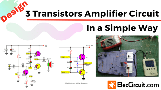
Today we are going to learn electronics by designing a 3 transistors amplifier circuit in a simple way. You will be able to design your own amplifier circuit with a driving power of 1W to 7W.
But if you want a higher driving power amplifier, you can do that without much inconvenience.
The objective of this article is just to learn, in the simplest way possible, about designing a power amplifier circuit. As a result, we will not be looking into in-depth calculations like power loss, component deficiency, and so on.
However, we hope that you find this article useful and that we can learn more together in the future.
Speaker and Amplifier Wattage
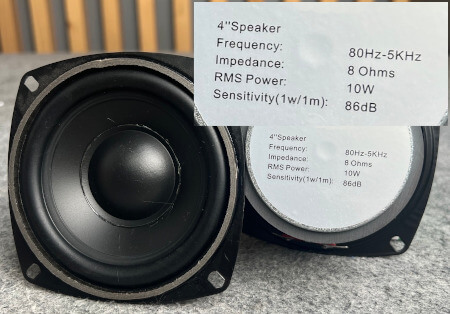
Suppose that we want to listen to music in a small room. We will be using a small speaker size of around 4 inches with a 10W RMS power and an 8Ω (Ohms) impedance, which is going to be more than adequate for our needs.
The 10W RMS power represents the sustained electrical power of 10W. In simple terms, the speaker’s rated wattage, or the amount of power it can withstand without distortion or overheating.
So we should also use a 10W power amplifier. However, to ensure the longevity of our speaker and to prevent distortion, we will only set the power amplifier to 7W, or 70% of the speaker’s 10W RMS power.
Suitable power supply
The determinant that affects the power that the speaker receives is the power amplifier receiving sufficient power from the power supply, both voltages and currents. Usually, we will consider the voltage first, so do this time.
Starts with defind:
P is RMS power.
V is RMS voltage.
We already know that P (power of the amplifier) is 7W and R (impedance of the speaker) is 8Ω.
Therefore, we should use the formula to find the power, which is:
P = V2 ÷ R
P = (V×V) ÷ R
V = 7.48V
And the amount of current we need:
I = P ÷ V
I = 7 ÷ 7.48 = 0.93A
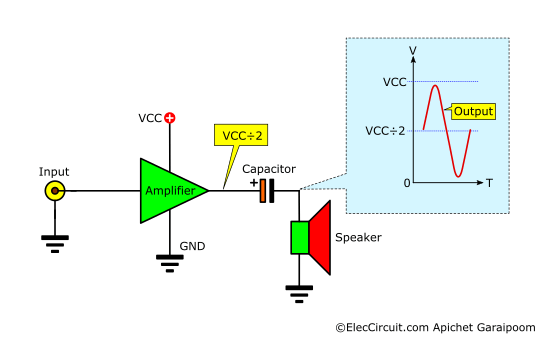
Since we want to learn about amplifier circuits in the most simple and basic way, we chose the OTL (output transformer less) amplifier circuit. But its main trait is that the output voltage will always be two times less than the voltage of the power supply.
That is why we are going to increase the power supply voltage to 14.96V (7.48V×2) to offset the losses.
Read more about Voltage, Current, and Resistance Relationship
RMS voltage
However, if we were to actually supply a 14.96V VCC (power supply voltage), the RMS voltage would be lower than what we wanted.
We can check if the amount of VCC will give us the RMS voltage we want by using this formula:
RMS voltage = 0.35 × Vp-p
We can roughly estimate that the Vp-p should be similar to the power supply voltage.
VCC = Vp-p
So if we try to plug the 14.96V VCC into the formula, we will get this result:
RMS voltage = 0.35×14.96V = 5.2V
And as you can see, it is significantly lower than 7.48V, which is clearly wrong. So what we could do is offset the VCC until we archive our desired Vp-p output.
We can find that offset value by rearranging the formula, as shown here:
VCC = RMS voltage ÷ 0.35
VCC = 7.48 ÷ 0.35
= 21.37V
Thus, in conclusion, we should use a power supply that is capable of supplying 21V and a current not lower than 1A so that the speaker can get an RMS power of 7W.
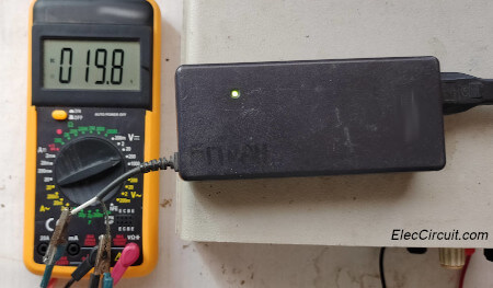
We chose this old laptop power supply with a size of 20V 3.5A, which is still in good condition and is enough for our usage.
Learn about unregulated DC power supply
Designing the Circuit
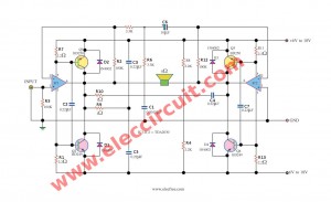
Next, let’s see the general circuit design we are going to use this time. As you might have noticed, the electronic circuit is quite similar to the Small Signal Amplifier Circuit. The Q1 is configured as a Class A amplifier, which has high gain but low working power.
So we add two more power transistors, Q2 and Q3. These two transistors work in a push-pull configuration, a Class AB amplifier.
Class AB amplifiers have an interesting point in that D1 and D2 need to be properly configured to bias Q2 and Q3.
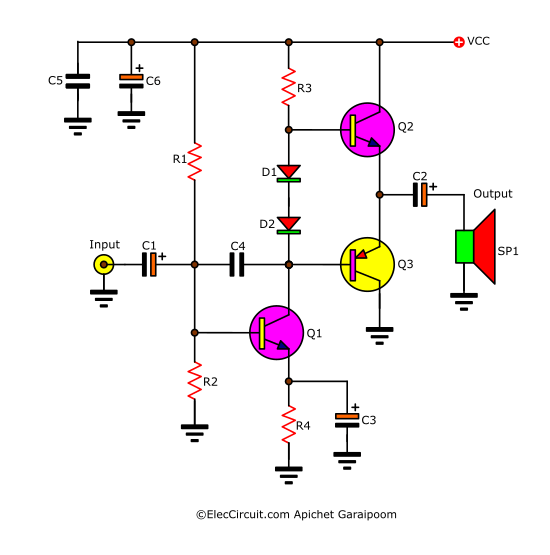
Picking Transistors
We can roughly assume that if we want the power of 10W at a voltage of 20V, we should go with the power transistors in the range of TIP41 (NPN) and TIP41 (PNP) in the package of TO-220.
We often use these transistors because they can withstand up to 4A of current, 40V of voltage, and a hFE of at least 30.
As for Q1, we pick S9013 (TO-92), speced as follows: IC = 0.5A, VCE = 30V max, hFE =100 min. Which is sufficient for us.
Our goal is to find the values of R1, R2, R3, and R4. We can do that through the principle that states that its resistance is equal to the voltage drop across it divided by the current flowing over it.
Therefore, we should determine or find the voltage and current at each individual point in the circuit first.
The Output
We will start with the voltage associated with the output first.
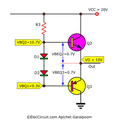
We already know that the VCC (input voltage) is 20V, and the VBEQ2 and VBEQ3 always stay around 0.7V.
And we know that the output voltage (VO) is half that of the VCC’s, which is:
VO = VCC ÷ 2
VO = 20V ÷ 2 = 10V
Then find the VBQ2 = VO + VBEQ2
VBQ2 = 10V + 0.7V
VBQ2 = 10.7V
Now we can find the VR3’s value, as shown:
VR3 = VCC – VBQ2
= 20V – 10.7V
VR3 = 9.3V
Next, we find the VBQ3 = VO – VBEQ3
VBQ3 = 10V – 0.7V
VBQ3 = 9.3V
The preamplifier
Then, we look into the preamplifier or small signal amplifier part of the circuit, as shown in the illustration below. And starts determining the voltage and current at each different point.
The preamplifier is a Class A common emitter, as described in our last article on this subject. You can learn more about them here: Designing Small Signal Amplifier Circuit.
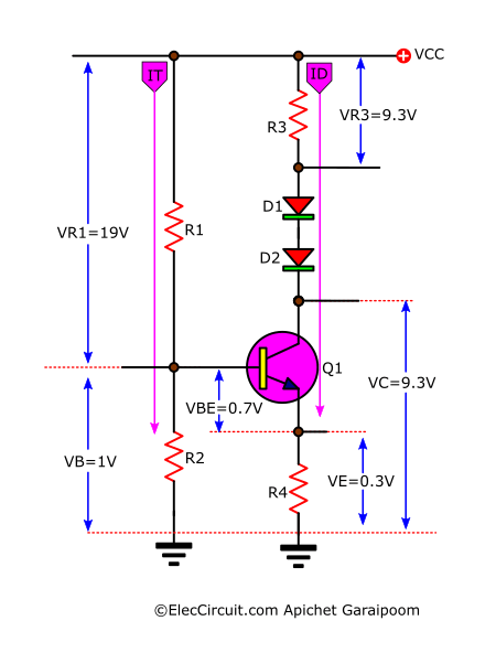
ID is 10mA; let’s start with ID first. The ID is the current flowing through R3, D1, D3, C-E of Q1, and R4.
Or, on the other hand, ID = IR3 = IR4 = 10mA
Furthermore, ID is a base bias current that flows through R3 and causes both Q2 and Q3 to function properly. The 10mA we have chosen should be enough for both transistors to operate and not so high that it would cause them to heat up.
Of course, if ID increases, so will the output. But it should not be too high, such as 30mA, 40mA or 50mA, since it will increase the current that flows through Q1.
So we would have to change it to a different transistor, like a BD139, which will have a lower hFE than the S9013. Apart from that, ID is a current that it loses all the time, causing the circuit to be excessively large.
IT is 1mA; It is a bias current that flows through R1, R2, and the Base of Q1. Normally, we would set it to be 0.1 times the ID.
It is enough for Q1, because when its hFE is higher than 100, its IB will be so low that it will not be able to influence the current flowing through R2 at all.
Therefore, IT = 10mA × 0.1 = 1mA , or in short:
IT = IR1 = IR2 = 1mA
VE (VR4) is 0.3V; it is a voltage that drops across R4 or VR4.
We try setting it to 0.3V, giving the transistor good gain and a wide operating range. We may also try changing it to other similar values, but it should not be too high because it will cause Q1 to not work properly and will affect VB and some others as well.
VB (VR2) is 1V; When VE is 0.3V, The VB or VR2 thus equal to VE + VBEQ1 or 0.3V + 0.7V = 1V.
VR1 is 19V ; Equal to VCC – VB or 20V – 1V = 19V.
Now that we are done determining the voltage and current in the circuit, let’s move on to the component, which starts with the resistors, because it is the easiest.
Finding the Value of Resistors
We will find the value of each individual resistor.
Finding R3
By R3 = VR3 ÷ ID
From VR3 = 9.3V, ID = 10mA
thus,
R3 = 9.3V ÷ 10mA = 0.93K
We will use 1K instead.
Finding R4
By R4 = VE ÷ ID
From VE = 0.3V, ID = 10mA
thus,
R4 = 0.3V ÷ 10mA = 30Ω
It will be 33Ω
Finding R2
By R2 = VB ÷ IT
From VB = 1V, IT = 1mA
thus,
R2 = 1V ÷ 1mA
R2 = 1KΩ
Finding R1
By R1 = VR1 ÷ IT
From VR1 = 19V, IT = 1mA
thus,
R1 = 19V ÷ 1mA
R1 = 19KΩ
We will be using 18kΩ instead.
About Capacitors
In the design of the circuit, we use the same train of thought as in the last article. So for the capacitors, we will not look too much into the way of finding their capacitance.
Since the principles are quite complicated, we instead try out many capacitors and see which one works best.
In practical usage, the difference is insignificant, and capacitors with similar values can be used interchangeably with one another.
So we chose the 10uF 50V for C1. The C2, which are both coupling capacitors, needs to respond well to low frequencies and have a low XC value to minimize the current loss in our AC signal.
We try using capacitors ranging from 470uF to 2,200uF, the difference is negligible, so we pick the 1,000uF 35V for C2.
The C3 is a decoupling capacitor that increases the gain in an AC signal and functions as if it were a very low-resistance resistor. We chose 47µF as C3.
C4 is a noise killer. A transistor amplifier circuit larger than 1W might require C4 to lower the chance of our circuit turing into a high-frequency generator or an oscillated circuit.
We can use anything from 22pF to 220pF, in this case, we will use 47pF 50V.
C5 will reduce voltage spikes or noise from the power supply. Normally, the noises have a very high frequency, more than 1MHz. The noise will think that C5 is a very low-resistance resistor, so it will flow through C5 to the GND.
C6 will keep the current smooth during high power usage. Like when we play very loud music abruptly and our amplifier circuit requires a high amount of electricity in a short period of time, causing the sound level to drop.
The C6 will function similarly to a tank, storing electricity and improving the efficiency of the circuit.
Read also: Capacitor working principle
Uses of capacitors | RC circuit time constant and Coupling
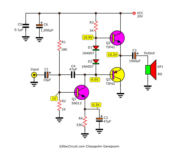
After we find the value for every component, we will get the complete circuit, as shown below.
Assembling the Circuit
Next, let’s assemble the circuit. My daughter chose to assemble it on a wooden plank, as usual. It is quite easy, even though it is significantly larger than using a normal PCB.
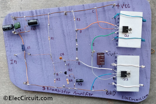
Component list
Q1: S9013, 45V 500mA NPN Transistor
Q2: TIP41, 100V 6A, NPN TO-220 transistor
Q3: TIP42, 100V 6A, PNP TO-220 transistor
Electrolytic Capacitors
C1: 10µF 25V
C2, C6: 1,000µF 35V
C3: 47µF 25V
Polyester or Ceramic Capacitor
C5: 0.1µF 50V
C4: 47pF 50V
0.5W metal/carbon film Resistors, tolerance: 5%
R1: 18K
R2, R3: 1K
R4: 33Ω
Read also: Electronic components list
Testing
First, after finishing assembling the circuit, recheck for any errors, such as the leads of transistors, diodes, electrolytic capacitors, etc.
Then, apply 20V from the power supply to the circuit and measure the voltage at each point, namely VO, VC, VD, VE, and VB. The results should be in line with what we have calculated.
The important point is VO; it should always halve the input voltage or 10V.
If VO has a significant change, for example, to 6V, it may be caused by the deterioration of Q3 or broken in a way that might leak between C and E. But if VO is higher than expected, like 13V, it might point to Q2 being deteriorated.
Normally, Q2 and Q3 need to be working simultaneously and in balance. Analogous to two resistors with the same resistance in series. Or in the form of the voltage divider circuit, causing their voltage drop across to equal or half that of the power supply.
But if one of the resistors has a decrease in resistance, it will cause its voltage drop across to decrease as well.
Next, we try to apply the input signal, speaking of which, this circuit requires an input signal with an amplitude of at least around 0.5Vp-p.
If the input signal is lower than this, the sound output will be inaudiable, and we would need to run it through a preamplifier first.
We tested it with a 1KHz sine wave signal, and the sound output sounds great.
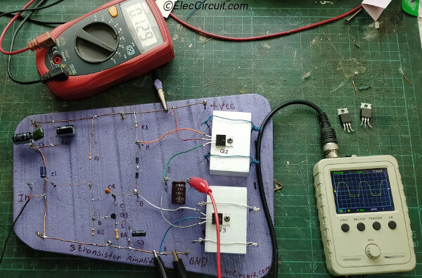
But if the input signal is too high, it will cause the output signal to have a distorted waveform. So when actually listening to the real music, it would be audiable but severely distorted. From our testing, the highest value without distortion is 15Vp-p.
Conclusion
We tested this circuit throughout, and it is quite usable. Proving that we can actually make a transistor amplifier circuit in a simple way, even though it is only suitable for a low-power output.
But if we want more power, we can switch out the transistors to the ones that can withstand higher power, increase the power supply, and increase the bias current of the transistors.
And we see that the quality of the transistors is very important, especially Q2 and Q3. They need to have as similar electrical characteristics (namely, hFE and IC) as possible.
Also, when we set a higher current and voltage target, the power loss within the circuit also increases. Currently, just the bare circuit, even without load, already requires around 100mA to operate.
If you are interested in this type of circuit or want us to go into a more complicated subject, please let us know.
GET UPDATE VIA EMAIL
I always try to make Electronics Learning Easy.

I love electronics. I have been learning about them through creating simple electronic circuits or small projects. And now I am also having my children do the same. Nevertheless, I hope you found the experiences we shared on this site useful and fulfilling.
This is wonderful. I just can’t wait to put my hand on and go through every step of the calculation relating to this design.
Thanks very much 🙏 🙏.
Hi, John
Thanks for your feedback. I am happy you like this post. If you finished it please it for us.
Have a great day.
Boa tarde .
Grato pelas iniciativas culturais até aqui .
Peço e agradeço , seja mostrado com igual simplicidade , o circuito que reproduziria dele o som 2.1 .
Como se fossem 3 circuitos desse sintonizados .
Seria Estéreo com reforço independente dos Graves .
Grato pela atenção !
Hi,
Thank you for your opinion. Next time, we will experiment with a bass-treble tuning circuit using RC. It was interesting learning about XC calculations. We think it will be useful for learning electronics. However, if the content is not what you expected, we apologize.
Why this? Arbitrary?
ID is 10mA; The ID is the current flowing through R3, D1, D3, C-E of Q1, and R4.
And this? Arbitrary too?
VE (VR4) is 0.3V; Voltage drops across R4 or VR4
How to choose if so?
Hi Kuwer,
First of all, I thank you for your question.
The concept for designing this circuit. We use experiments and make predictions based on our prior knowledge. ID initialization is important and VE has a lot to do with circuit performance.
Of course, this circuit may be more efficient. Suppose using the most appropriate equipment value. This will be the next step of our learning.
In conclusion, we test to meet the results (various voltage points) and the device does not get too hot according to available resources.
Thanks again.
Apichet
Ok. Thank you.
Bom dia Apichet !
Peço e agradeço , se oportuno , voltar ao meu questionamento de 9 de maio sobre o áudio 2.1 .
Só você ou a sua ordem com tanta informação , pode a mim e a outros ajudar a esclarecer essa esquecida arquitetura .
Será que é porque não tem expressão comercial ?
Good evening
First of all, I apologize that I may not be able to answer all your questions because I am not an expert on amplifiers. I made very little of it. Because of past experiences, My family (my mother) doesn’t like high-wattage amplifiers. because of the loud noise So I don’t have much experience with it. But I like learning about electronic circuits.
As for the 2.1-channel amplifier, I haven’t seriously tried building one yet. For now, we will focus on learning simple electronic circuits.
Is this a post? https://www.eleccircuit.com/simple-delay-speakers/#comment-359706
Thank you for visiting the website and your support.
God bless you.
Hey,
I’m finding your simple circuits really useful and informative to learn about electronics, keep up the good work!
I’ve built this amplifier on a breadboard and it sounds pretty good. However, I have a serious problem with it as it is burning out the output coupling capacitor (C2): literally, they’re hot, the tops are starting to bulge and one even went pop!
Any ideas or suggestions? The test voltages are pretty close. I measured the hFE of Q2 & 3 (TIP41/42) and they aren’t very close: 98 & 124. Is that a problem?
Any help would be appreciated, I’d like to sort it out so I can get it on a permanent strip board for use.
Hello,
First of all, thank you for your interest in building this circuit. It is very suitable for learning simple audio amplifier circuits.
But I’m a bit saddened that you can see the results of capacitors like this.
I would like to share my experience with Electrolytic capacitors. It will not withstand voltage levels higher than specified and if connected to the wrong polarity, it will be damaged as well.
In this article, I admit my mistake. There is no component list: because I thought we had suggested this. There are many articles such as: https://www.eleccircuit.com/what-is-capacitor-principle-working-types/#Electrolytic_Capacitors
Hope this experience Might be useful for you.
I sincerely apologize for wasting your time.
Thanks for your quick reply.
You’re not wasting my time 😀: I’m learning and blowing up the odd capacitor is part of the fun 😉 (always wear safety glasses !)
I think I may have spotted the problem? On the 2 schematics the polarity of C2 has negative connected to the output of Q2/3 and positive to the speaker+, Is this an error?
The first simpler diagram has it the other way round, as it is also on the TIP41/42 version of your 4 transistor amp: https://www.eleccircuit.com/4-transistor-audio-amplifier-circuit/
Hi,
Great! My kids don’t really like wearing eye protection. It may be dangerous from those accidents.
That’s right. Current will always flow through the transistor, through the capacitor, to ground through the loudspeaker (load), so it will always receive positive voltage first.
Have a good day,
Hi again,
I’ve built this amplifier up on stripboard, attached a sizable heatsink and put it in a nice box. I’m running a Bluetooth card into it and driving an old Aurotone speaker. It sounds great, I love it’s sound.
The only problem I have is that if I leave it on, but not playing music, it gets very hot. I can play music quite loudly for hours, the heatsink is warm but the outer casing remains cool to touch; if I leave it idle for 10-20 minutes the casing is very warm and, upon opening it, the heatsink is too hot to touch!
Any insights or suggestions would be appreciated.
Still loving this little project 😁
Hi,
I am glad you had a great experience. I can see the atmosphere of listening to soft music in the room and sipping hot tea in the afternoon, it is one of the joys of us electronic amateurs, right? 🙂
God bless you,