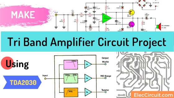
This is a Tri audio amplifier circuit. Why it is interesting?
Imagine, how well do we know. If you hear the music of the full frequency band in our cheap audio system.
This project maybe great answer.
The tri audio amplifier has three in one a amplification act drive specifically each audio speakers. It makes the sound quality is very good.
In Normal amplifier can drive three speakers at the same time are the woofer, mid-range and tweeter. Which may have limits. For example: the impedance of the speakers, the loss of signal in Crossover Network. But it’s very expensive.
Thus, when compared to the same quality and power of these amplifier and crossover network. They will have the price more than this the Tri audio amplifier circuit.
When viewing the various elements, then are seen as better in every aspect.
Although there are not a lot of power. But it’s only for listening in your home or bedroom very well.
Some people are interested in the efficiency of this circuit. See in the graph below.
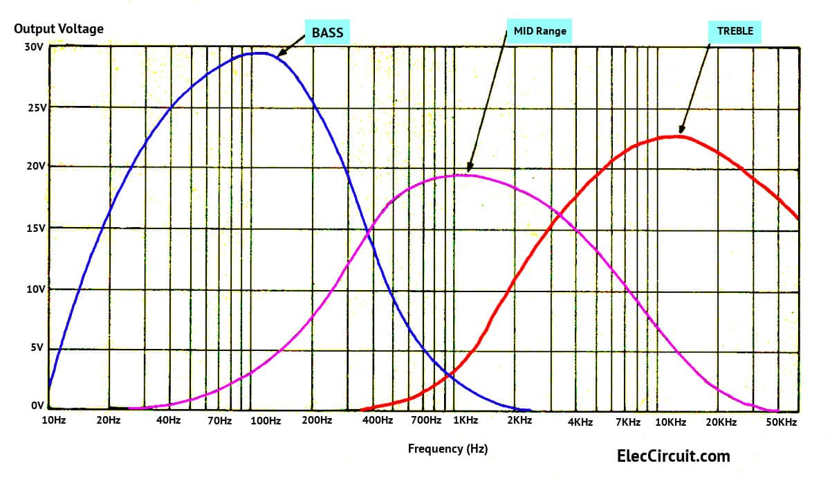
We will see that it can respond to the sound frequency well. Covering almost all frequency bands
You probably got the answer. Are you ready?
The working principles
Look at the below.
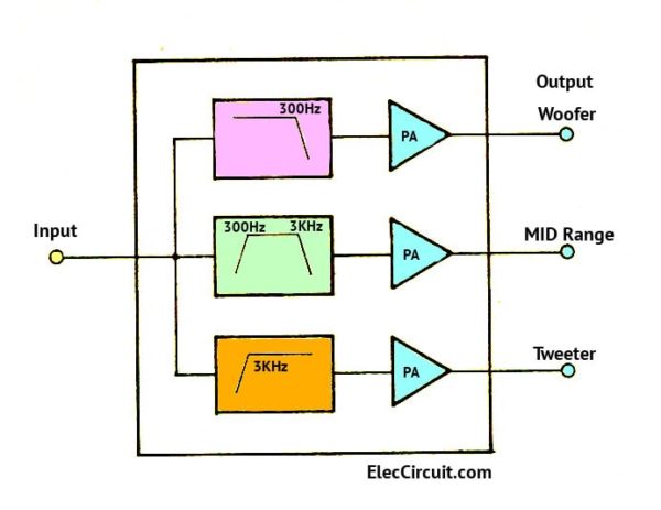
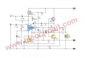
It is a block diagram of tri audio amplifier circuit. It will split the audio frequency range into 3 ranges:
- Cut off at 300Hz for low frequency range.
- Then cut off at 3 KHz for midrange.
- And the frequency exceeds 3KHz is the high frequency.
Then the signal is sent to each audio amplifier circuits. To drive each speaker the woofer, midrange and tweeter immediately.
What is more? see circuit!
How this circuit works
Look at the complete circuit diagram below.
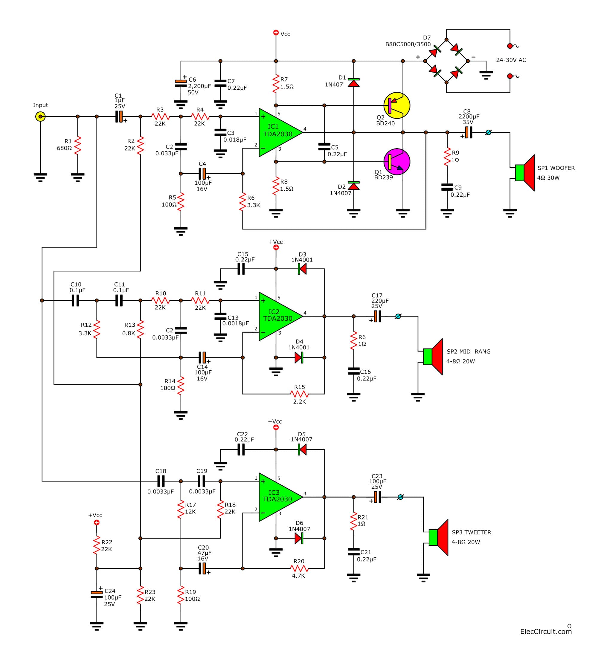
Although many devices. But probably easy. If gradually understanding it. Here is step by step a process.
Recommended: TDA2030 Audio Amplifier Circuits
The Woofer or Bass sound
The resistor R1 will be connected between input and ground. To control input signal does not too much. And makes a constant impedance input.
The C1 act as coupling the input signal to a low pass filter circuit.
Which they consists of R3, R4, C2 and C3. The signal that through this filter circuit will be low frequency under 300 Hz only.
Then, this signal comes to input of IC1(TDA2030) to amplify. To the drive transistor Q1 and Q2. They increase the audio up.
And Both resistors R7 and R8 are biased to Q1(BD239) and Q2(BD240).
The resistor-R6 is feedback. And both C4 and R5 are divider the feedback voltage too.
Both R9 and C9 are load for this section circuit. The capacitor C8 act as coupling output signal to drive the woofer speaker.
Read Also: TDA2030 transistor amp circuit with PCB
The MidRange Sound
The middle sound frequency are about 300Hz – 3KHz. It will pass the mid rang filter circuit.
Which they consists of C10,C11,C12 and R10,R11,C12,C13. Both is filter 2 step in series together.
Then, this signal comes to the input of IC2. To increase the power up.
The R15 is the feedback. And R14,C14 are the divider feedback.
The R16,C16 are load of circuit.
The C17 act coupling the output signal to the Mid-rang speaker.
What is more? See!
The Tweeter or Treble sound
And in high frequency range that exceeds 3 KHz. It will pass the high pass filter circuit. They comprises C18,C19 and R17.
Then this signal will come to the input of IC3. Which it act as amplifier the signal rise.
The R20 is a feedback. And C20,R19 are divider a feedback voltage. The R21,C21 are loadof circuit.
The C23 act as coupling the output signal to drive Tweeter speaker.
The R22 and R23 are connected as the divider circuit. To separate the voltage to half of the power supply circuit. And C24 maintains the voltage to smooth and constant.
This voltage is a biased the voltage to the input (pin 1) of IC1, IC2 and IC3.
Read next: TDA2030 stereo amplifier circuit
Protection and power supply
And R2, R13 and R18 limit the current is not too much.
Diodes D1-D6 protects the IC from damage from the feedback voltage .
The capacitors C7, C15 and C22 helps eliminate noise from the power supply.
The C6 filter to smooth the power supply circuit. And diode D7 is a diode bridge rectifier of the AC.
Let’s build this circuit
This project is quite easy, since we use popularly components. As shown in PCB layout diagram.
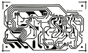
and
Components layout
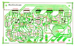
The components layout of Tri audio power amplifier
I trust you can make them.
Parts you will need
0.25W Resistors, tolerance: 5%
- R1: 680Ω 0.5 watts
- R2, R3, R4, R10, R11, R18, R22, R23: 22K
- R5, R14, R19: 100Ω
- R6, R12: 3.3K
- R7, R8: 1.5Ω 0.5 watts
- R9, R16, R21: 1Ω 0.5 watts
- R13: 68K
- R15: 2.2K
- R17: 12K
- R22: 4.7K
Electrolytic Capacitors
- C1: 1µF 25V
- C4, C14: 100µF 16V
- C6: 2,200µF 50V
- C17: 220µF 25V
- C20: 47µF 16V
- C23, C24: 100µF 25V
Ceramic or Mylar Capacitors
- C2: 0.033µF 50V
- C3: 0.018µF 50V
- C5, C7, C9, C15, C16, C21, C22: 0.22µF 50V
- C10, C11: 0.1µF 50V
- C18, C19: 0.0033µF 50V
Semiconductors
- D1-D6: 1N4001, 50V 1A Diodes
- BD1 or D7: 5A 200V Bridge Diode
- IC1- IC3: TDA2030A
- Q1: BD239, TIP41, 40V 4A NPN Transistor
- Q2: BD240, TIP42, 40V 4A PNP Transistor
Others
T1: 24V to 30V 3A transformer
PCB, Heatsinks, transformer
Here are a few related posts you might want to read:
- LM3875 Gainclone Amplifier circuit | Stereo 56W
- LM1875 Datasheet 30W HIFi audio amplifier circuit
- Cheap car subwoofer filter circuits
Related Posts

I love electronics. I have been learning about them through creating simple electronic circuits or small projects. And now I am also having my children do the same. Nevertheless, I hope you found the experiences we shared on this site useful and fulfilling.
Pls how much wattage can this circuit provide?
Look on the circuit 70 watts each channel
How can i buy this board?
Why gone pictures “As shown in PCB layout diagram. and Components layout” ?
Hello Audrius Lazauskas,
Thanks for your interest in this circuit. I sent these PCB layouts and components to your email.
Thanks
Hello, The circuit seem to be so cool but what if I want to adjust woofer, mid range and treble?
You may change the RC network at the input section. They will change the frequency filter.
I am excited about your experiment. 🙂
Hello i tried the circuit and i start with the woofer one, i use the transistors TIP 41 and 42 but i don’t know why its overheating even if i fix it with heatsink and i use all the required components and i just test it with 12v only plzz help me on this.
Hello the transistors in a woofer circuit are over heating i use tip 41 and 42 pls what can i do
Thanks for your visit to my site again.
I am really sorry this circuit get a mistake too much. I draw it new. (R8 is 1.5 ohms) Please forgive me! 🙂
I am not a designer of this circuit. But I think this circuit is interesting, you too?
If you use only a 12V power supply. It may be too low for this circuit.
Hello.
Where is the printed circuit?
Can you send it to me?
Hello Mesut,
Yes, you can.
I send PCB layout to your email.
Thanks
thanks for your good job but please i need the pcb files can you send it to me please?
thanks
yakout
Hi YAKOUT
I send the PCB layout to your email.
Thanks
PCB layout and components layout is not clear. I wish I could build and try this circuit. Could you send me clear layout by email please.
Two more questions…
(1) If the specified transistors are not available, can I replace with another pair which may be available in local market? If yes, which would be appropriate?
(2) Can I use bridge configuration for the Bass channel? If yes, what alteration would you suggest in other components?
I need pcb layout please.
Hi,
Just now we have sent the PCB layout already.
We apologize for the delay.
I and my dad hope you finish it and have a good sound. 🙂
Hello can i get the pcb lay out too. thanks🙏🙏🙏
Hi,
I’m glad you’re interested in making this circuit. I want to make this circuit too, but at the moment it seems a bit difficult for me. Dad said that I need to wait to learn more about Electronics to be able to make this circuit. However, Hope you to be able to build it successfully, I just send you email PCB layout. Wish you success and good luck. 🙂
hi could you send me a clear pcb lay out of both sides so that i can download and work on this project..? i really want to try it.thanks
Hi,
Just now we have sent the PCB layout already.
We apologize for the delay.
I and my dad hope you finish it and have a good sound. 🙂
Thanks for sharing even I came in late. please are you in a position to send me PCB files on my email, I will certainly appreciate.
Hi,
Just now we have sent the PCB layout already.
We apologize for the delay.
I and my dad hope you finish it and have a good sound. 🙂
Can i have the component and pcb layout please?
Thank you!!
Hi,
Just now we have sent the PCB layout already.
We apologize for the delay.
I and my dad hope you finish it and have a good sound. 🙂
Hi, I’m interesting this circuit and want to try. Can you give me PCB layout?
Thank you.