If you are looking for a constant frequency generator that easy and inexpensive.
Here are the transistor crystal oscillator circuit ideas. They may help you works finish.
There are 4 circuits as follows.
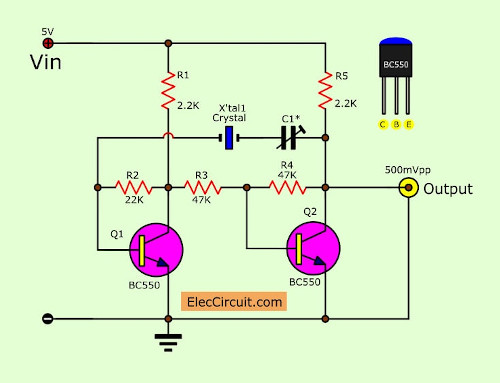
1# Carrier wave generator circuit
25 years ago, I used this oscillator circuit to AM radio station. I use it like a radio frequency carrier with 639kHZ Crystal. The below circuit works perfectly.
Read next: Crystal tester circuit with PCB
Note:
- C1 is trimmer 2-30pF
- You can use any crystal, for example, 100kHz to 10MHz.
- The output is sine waveform about 0.3-0.5Vp-p.
- The power supply voltage is 3V to 12V regulated supply.
Here is a full article of AM carrier frequency. Look at the circuit below.
Before reading the details in the circuit section. I want to tell the story of this project first. If bored, just skip it.
My friend works at an AM radio station. He said the device was broken. Because of lightning. At the frequency carrier circuit.
He therefore borrowed from another station to use temporarily. But it doesn’t work well. Because the frequency is too changed. In principle, the value should be changed no more than 10%. But this changed approximately a hundred hertz.
Which exceeds the set standards His boss said that he had ordered a new device. But need to wait about two months
So, He consulted me. Can I build this circuit?
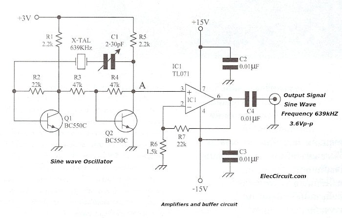
The main feature is that it can produce a sine wave frequency of 639,000Hz or 639.000 kHz. And the amplitude range of 3 Vp-p to 5 Vp-p.
What is a carrier wave?
It is the signal that is mixed with an audio signal. To be used to transmit the sound signal through the antenna distributed into the air to the receiver. Considered that this carrier wave is very important. And must be accurate as specified. To not disturb the channels of other stations
How to get the circuit
We know that crystal sets the frequency very precisely. I guess that the crystal on the same device would not be damaged by lightning.
So remove it to check with the crystal checker circuit. It turns out that it’s still normal.
Then, we get the circuit as above is like transistor astable multivibrator. I try to change the parts until getting the best.
Recommended: Learn transistor circuit works here
Do you notice? In the sine wave oscillator section. It has a few parts. And, important without the capacitors. But it can generate a frequency easily. Why?
From what I know Between the joints inside the transistor like a very small capacitor is hidden.
We can use R2 and R4 to determine the waveform. Then, I tried using an oscilloscope to measure various points.
It appears at point A has to get the perfect sine waveform. And get a voltage of approximately 0.5Vp-p
Do you wonder why we do not increase the power supply voltage? To increase the output voltage as scheduled.
But I got bad results. And change to R1, R5, it also appears distorted waveforms.
Therefore, we better amplify the signal later.
After that, I measured the frequency, there was also a slight discrepancy. Then I tried using a trimmer to connect the series with the crystal.
According to the idea that a crystal has properties similar to a small capacitor.
It appears that we can adjust the frequency a little until the frequency value meets the needs.
Non-inverting Amplifier
Next, we need to find a circuit that acts to increase the voltage and become a buffer. When connecting with the transmitter It will prevent malfunction and damage of this frequency generating circuit. So, It gives the wave shape that doesn’t change.
I think that the right equipment is the op-amp buffer(Non-inverting amplifier). I chose TL071, High-frequency low noise op-amp. It is easy to connect the circuit and can buy any store. In addition, I tried the LF351 but the signal was distorted.
I experimented with the circuit, changing R6 and R7. The amplitude increased to about 3.6Vp-p. And the waveform was the same. Which is considered to be a good use.
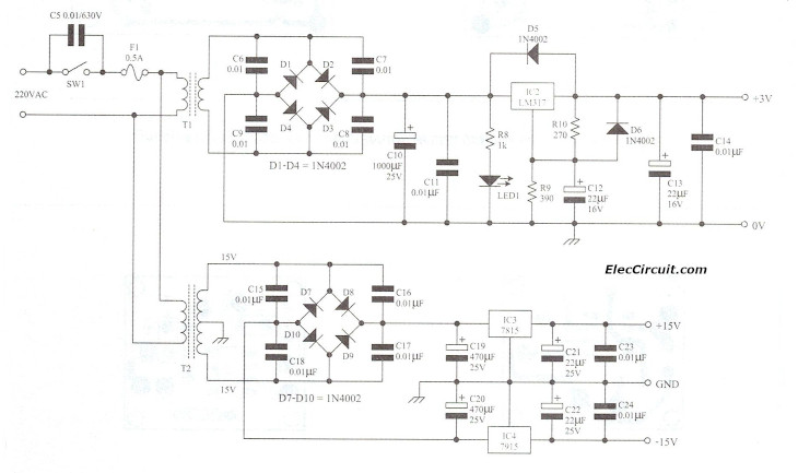
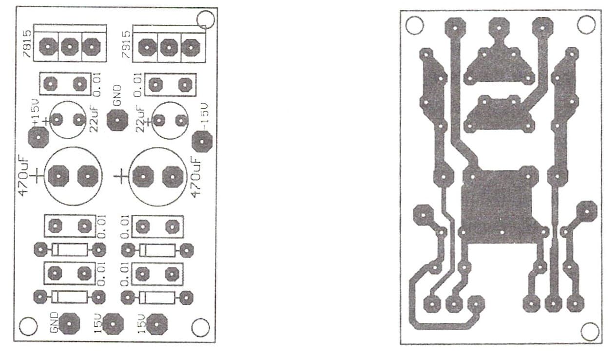
Power supply
For the power supply sector of the frequency generator circuit and the amplifier buffer.
Although this circuit uses very little current. We can use Zener diodes and transistors. But for convenience. I choose to use instant IC.
I also use IC No. LM317T for 3V power supply and No. MC7815 and MC7915 for power supply + 15V and -15V respectively.
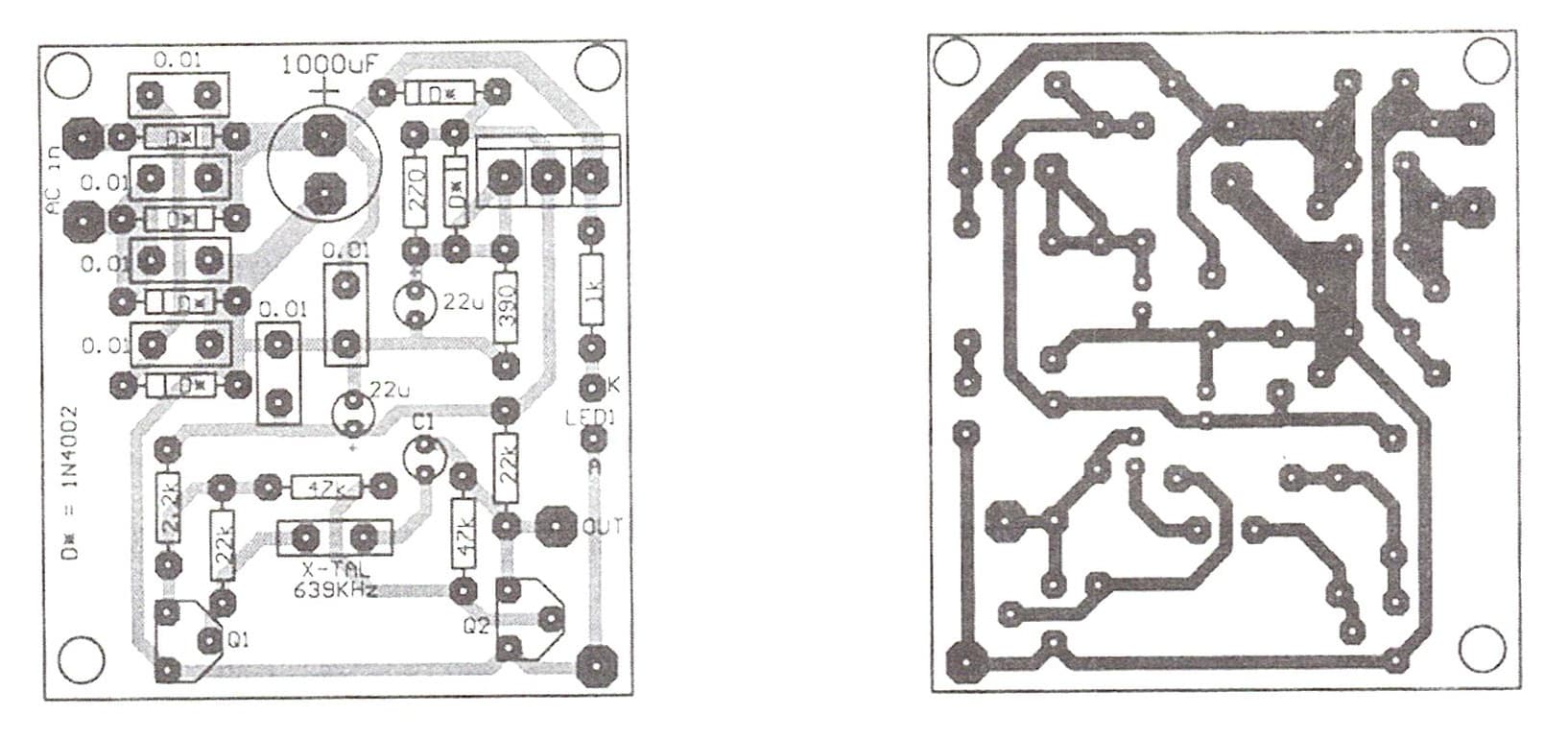
How to build
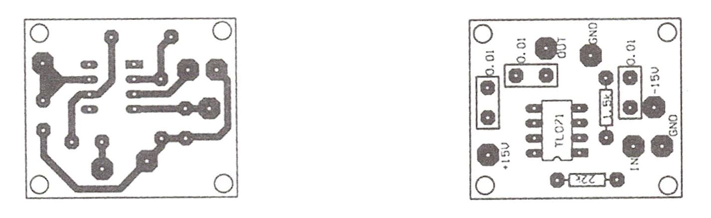
This project we can assemble them on the universal PCB. Or we can build a PCB as an example below.
Then, look at the Prototype below. I assemble it in metal boxes to protect some noise. Next, I measure the frequency is 639.001 kHz.
It only has a 1 Hz discrepancy.
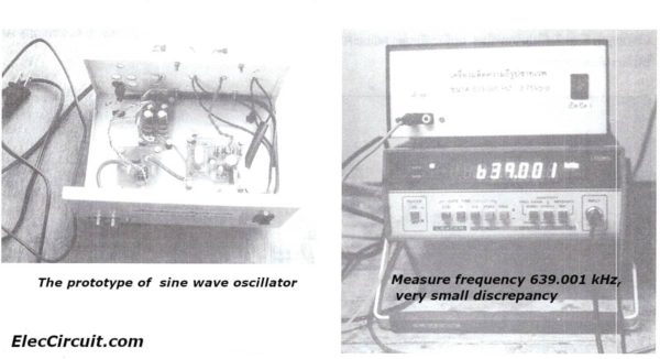
My friend put it to the test, for two months have worked well.
Also, Other transistor oscillator circuit ideas for you. Though very ancient and easiest, they still have many uses.
Read next: Based time crystal clock generator circuit
2# Oscillator astable multi-vibrator with Crystal controller
An oscillator circuit of this nature. Often used as a clock circuit. This circuit uses a million crystal frequency control with stability.
And a circuit that does not use the capacitor or Inductor all.
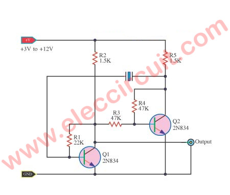
Each transistor to work, the amplifier with feedback. The Q2 transistors(2N834) to circuits with a gain equal to 1.
The gain of the transistor Q1(2N834), as a function of the resistance of the crystal, while the resonance.
By default, the resistance will be less than 22K. This is the feedback resistance of the circuit.
Therefore, the gain of the circuit Q1, it is higher than one.
The Output from a square wave circuit. The size of the signal depends on the voltage input to the circuit. This circuit can oscillate from birth 3 kHz up to 10MHz.
On a long time ago I’ve used this product on a standard radio frequency AM 639KHZ can work well.
The output signal is a sine Very low distortion. But the temperature should be carefully stable.
Here are a few related posts you may find helpful, too:
- Sine wave generator circuit with double balance mixer IC
- XR2206 function generator circuit
- Simple IF signal generator circuit using CMOS IC
3# Low voltage crystal oscillator Circuit using FET
We can easily use FET and Crystal to generate the frequency as Low voltage crystal oscillator Circuit, 1.5V-10V supply.
It can operate at a supply voltage to 1.5 volts only and at crystal frequency 100 kHz to 10 MHz.
The crystal is connected to between the drain and gate of FET-T1 BF256. It runs in resonance mode in parallel coil form.
The inductor L1 makes better frequency stability and can use crystal in the wide frequency range, Although the crystal is not appropriate, it also works.
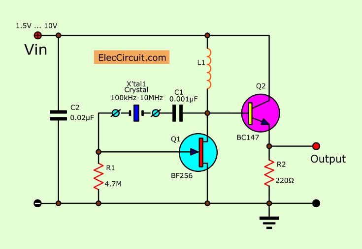
The capacitor C1 is connected with the crystal to act as “padding” for the return phase 180 degrees, to the input of FET. The output will be buffer by T2.
This designed circuit is tested to operate at frequencies 100 kHz, 1 MHz, 4 MHz, 8 MHz, and 10 MHz at the lowest 1.5 volts only.
Parts you will need
T1: BF256 FET transistors
T2: BC147 NPN Transistors
C1: 1nF 50V (0.001uF) Ceramic capacitors
C2: 22nF 50V (0.022uF) Ceramic capacitors
X’t: 100K-10MHz Crystal
R1: 4.7M 0.25W resistors
R2: 220 ohms 0.25W resistors
Recommended: 60HZ CLOCK Pulse Generator using MM5369
4# Symmetrical Harmonic Oscillator circuit
Here is another one of the transistor crystal oscillator circuit ideas. This is the Symmetrical Harmonic Oscillator circuit. It generates 3rd harmonic frequency using the crystal.
This special circuit is without a tuning circuit. Because these type circuits always use a tuning circuit.
How it works
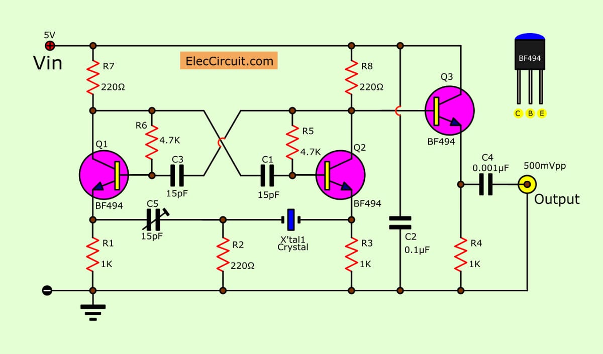
In the circuit diagram below is the astable multivibrator Oscillator circuit. There is the crystal across both emitter lead of transistors Q1 and Q2.
The 40pF trimmer capacitor-C5 connects with crystal to adjust the fundamental frequency to get 3rd harmonic frequency as you want.
This circuit is designed for the crystal that uses the fundamental frequency of 6-20 MHz. The output frequency of the circuit is between 18MHz to 60 MHz.
You can use the normal RF transistors can in this circuit. The output has a signal of about 500mVp-p. That is enough for common usage.
Check out these related articles, too:
- 5 Crystal oscillator Circuits using CMOS
- Sine wave oscillator low frequency-constant amplitude
- Variable Time base oscillator circuit by cmos IC
GET UPDATE VIA EMAIL
I always try to make Electronics Learning Easy.
Related Posts


I love electronics. I have been learning about them through creating simple electronic circuits or small projects. And now I am also having my children do the same. Nevertheless, I hope you found the experiences we shared on this site useful and fulfilling.
This Is Handy!!!!!!!!!!
Hi MR OHM 1970
Thanks for your feedback.
Hello everyone,
what is the value of the self for a crystal of 100KHz
thank you.
Yes, the lowest crystal is 100 KHz.
Hi
Sorry, i am beginner in electronic. My question is, How can i produce square wave with the first circuit? (I mean: Transistor Crystal Oscillator circuit ). Please note that, i don’t want use Schmitt trigger ICs.
Thanks
Hello Alireza F.
Thank you for visiting the site. I cannot explain to you how it works, now. I am busy. I am sorry.
I hope you still learn electronics more. It makes your skill grow up. I believe you.
I used the first circuit and it did not work. A complete waste of time and a bit of money.
Hi Mouka,
Thanks for your feedback. I am sorry to hear that.
Somethings may be wrong.
I did this circuit. It is worked well.
Hi, i built it but only work for one crystal , and the f=450 Khz
I built circuit #1 .I did not have the 639kHZ Crystal or the BC550 transistor. With this circuit I made some interesting discovery’s . I started by using a 32Khz Crystal and two BC547 transistors both of which I have in abundance. I was able to obtain a near perfect sine wave at slightly above 32 Khz . I then changed both transistors to the 2N2222 with a variety of fixed capacitors this provided a perfect sine wave with over 1 volt in amplitude.
It also worked with a 10K resistor replacing the capacitor which also worked. I then obtained a decent square wave replacing the crystal with a resistor and capacitor in series. I found that the circuit as simple as it is can produce a variety of wave forms with many different components by mixing or changing the NPN transistors I obtained a variety of results. I have some FET op amps to work with bringing the signal to the rail . I have a wide variety of FET’s to work with the circuits that follow this one . Thank You for providing these free designs for all to use . There is a wealth of knowledge here for anyone with an interest in electronics . I hope more people benefit from it as I have.
Hello Paul Burns,
Thanks for your visit to my site.
It is so great. I love your text. I have made me smile. I also like to try many circuits.
I believe your message is useful for many friends.
I built this crystal oscillator circuit for a friend a long time ago. And I’m glad it worked out well, in low-frequency crystals too.
FET is also an interesting device for testing the oscillator circuit.
์New discovery by ourselves It was a joy and an impression.
But lately, I’ve been very busy. We’re moving house. From the city to the suburbs (rural). Because it takes a lot of money to build a new house. So we build ourselves.
It is nice to meet you. Mr. Paul Burns.
Have a great day.
Thanks for putting in all this work. I tried two BC547’s for #1 because that is what I have.
I also found some differences using two 2N2222’s . I also got a fairly decent square wave by replacing the crystal with a capacitor and resistor in series. Duty cycle was off but can be adjusted. Very nice sine wave with original design. There’s lots more but my first post was considered spam i guess because it was two paragraphs. Looking forward to more work on this and other circuits. Thanks !!!!
Your text looks great. Thanks for your experience. It is good for the hobby.
Entering the imagination of learning. Finding out what we are really interested in. It was a time of happiness.
Thanks a lot again!
On circuit #3 I did not have the BF256 so i tried a variety of other JFETs . The J111 worked the best . I was also able to get the circuit working well with the 2N5245, and the BF245 . All are listed as N-Channel JFET RF amplifiers . The J111 is also used as a chopper or modulator. I will try others as well . These are listed as depletion mode devices .They are normally conductive between the source and the drain terminals with no connection to the gate terminal. If the gate is grounded through a resistance as in this circuit they will stop carrying current between the source and drain terminals . When a more positive voltage is applied to the gate the device will start conducting current between the source and drain in relation to the value of the voltage applied to the gate .They are considered to be voltage controlled devices .The connection of the capacitor and crystal between the gate and drain with the inductor allow the crystal to resonate at its designed frequency in a feedback loop. I was able to use a frequency counter and oscilloscope to prove the oscillation of several different frequency crystal’s with this simple circuit to the exact frequency’s . The NPN transistor provides amplification . Again I substituted as i did not have the listed component . I used the H10 ,2N2222, and trying others as well . Just make sure that you review the spec sheets to make sure that you have connected all the transistors as different transistors have different pin locations. Thank You
Hi Paul Burns,
Thanks for your sharing. It is so great.
I’m glad you discovered a new challenge.
You are very brave. Some circuits I haven’t tried yet. So it has an error. I’m so sorry.
Your sharing is very helpful to others.
Have a great day,
Apichet
Hi, thank you for clear explanation. Can I use the oscillator circuit using BJT in modulation part, instead of using OPAMP?
Hello Tigreal,
Thanks for your visit to my site.
Sorry, I can’t confirm. It’s an interesting concept. I haven’t used it yet. If there’s a chance, I’ll try it out.
Thanks