Let’s build an XR2206 function generator circuit. In the past, finding a function generator could be expensive—a big hassle per se. But nowadays, you can build one yourself easily with a couple of ten bucks on hand. Consider it; isn’t it interesting?
At the working heart of this circuit is an XR-2206 integrated circuit. It is a popular function generator capable of producing high-quality sine, square, triangle, ramp, and pulse waveforms of high stability and accuracy.
XR2206 Function Generator
Basic Feature
- Can generate sine/triangle/square waveforms.
- Frequency range: 1Hz-1MHz.
- Adjustable frequency and amplitude.
- Can apply it to a TTL circuit that uses 5 volts.
- Frequency adjustment features coarse tuning and fine-tuning.
- And more.
Feature of XR2206
- Wide Supply Range, 10V to 26V
- Low-Sine Wave Distortion, 0.5%, Typical
- Excellent Temperature Stability, 20ppm/°C.
- Wide Sweep Range, 2000:1
- Low-Supply Sensitivity, 0.01%V.
- Linear Amplitude Modulation
- TTL Compatible FSK Controls
- Adjustable Duty Cycle, 1% TO 99%
We can apply it for other applications.
- Frequency Waveform Generator
- Phase-Locked Loops (VCO)
- Sweep Generator
- AM/FM Generator
- V/F Converter
- FSK Generator
XR2206 Pinout
See the pinout and pin detail below.
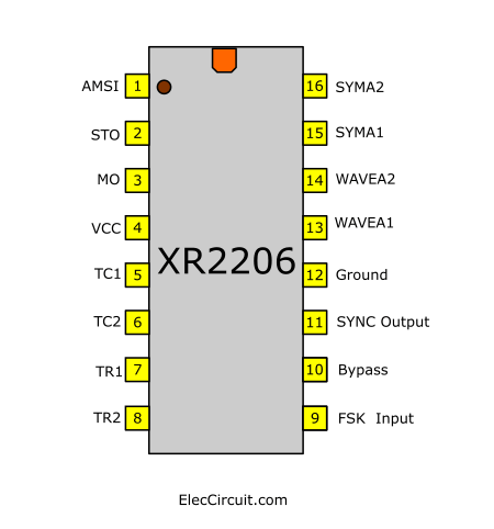
PIN DESCRIPTION
1 AMSI: Amplitude Modulating Signal Input.
2 STO: Sine or Triangle Wave Output.
3 MO: Multiplier Output.
4 VCC: Positive Power Supply.
5 TC1: Timing Capacitor Input.
6 TC2: Timing Capacitor Input.
7 TR1: Timing Resistor 1 Output.
8 TR2: Timing Resistor 2 Output.
9 FSKI: Frequency Shift Keying Input.
10 BIAS: Internal Voltage Reference.
11 SYNCO: Sync Output. This output is an open collector and needs a pull-up resistor to VCC.
12 GND: Ground pin.
13 WAVEA1: Wave Form Adjust Input 1.
14 WAVEA2: Wave Form Adjust Input 2.
15 SYMA1: Wave Symmetry Adjust 1.
16 SYMA2: Wave Symmetry Adjust 2.
And, the inside of this IC can be divided mainly into four parts, as follows:
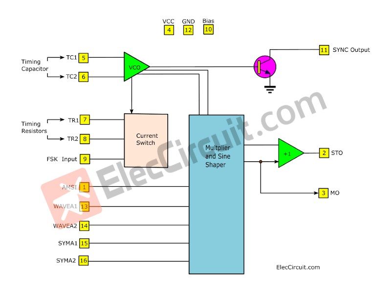
How does it works
Voltage-Controlled Oscillator (VCO): This gives out a frequency depending on the capacitor connected between pin 5 and pin 6 and the resistor between pin 7 and pin 8. The output can be achieved in two ways. The first is sync frequency or square-wave output. whereas another way is to run it through a sine-shaper circuit. Which led us to—
Sine-Shaper Circuit: It will create for us a sine-wave or triangle; adjust by changing the resistance of the resistor between pin 13 and pin 14.
Buffer Circuit: Works by keeping the output’s impedance low; helps when connecting to other circuits.
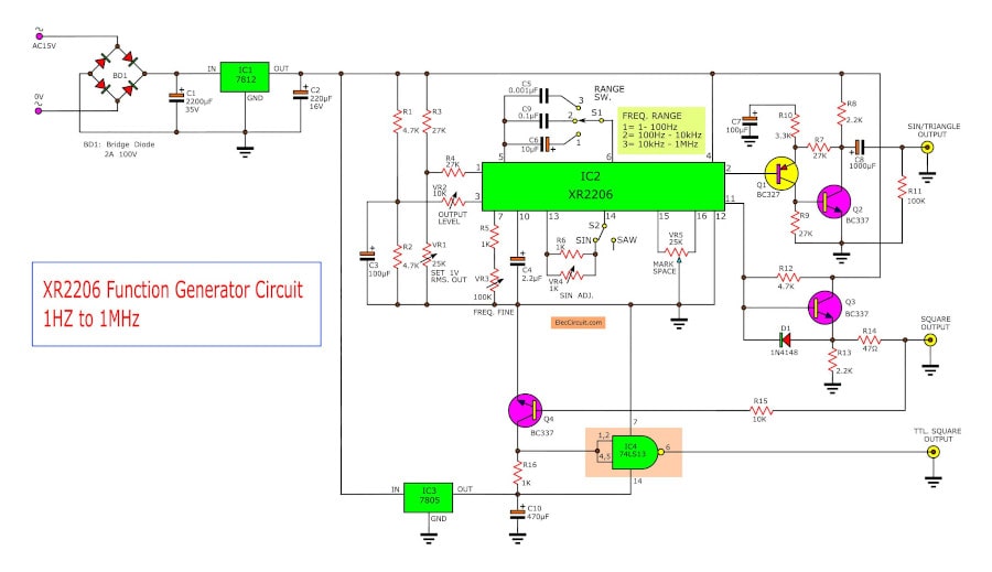
In the actual circuit shown below, we might see that the switch S1 acts as a frequency range selector. The three choices are:
1. 1-100 Hz
2. 100-10,000 Hz
3. 10,000-1,000,000 Hz
Nevertheless, fine adjustment for all three ranges is achievable by changing the impedance through VR3.
The VR2 is an adjuster for the gain of the circuit; adjusting it in conjunction with the RV1 gives a maximum output of 1 volt.
As for VR5, it’s there for tuning the stability of the wave signal. The switch S2 allows us to choose the output between a sine-wave or sawtooth signal.
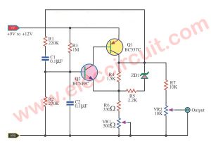
The output signal will then get sent through a buffer circuit consisting of Q1, Q2, and ultimately C9. But for the square wave output, it will come out of pin 11 and be fed to a transistor buffer circuit. The output will be at the emitter.
The square wave signal will be around 12 volts peak to peak; therefore, if you perhaps want to apply it to a TTL circuit that uses 5 volts, you would have to add a simple converter circuit using SN74LS00 from below.
The Components list
IC1: LM7812,12V DC voltage regulator
IC2: XR2206 Function Generator
IC3: LM7805 5V DC voltage regulator
IC4: SN74LS00 Nand gate IC TTL
Q1: BC327 50V 800mA PNP Transistor
Q2, Q3, Q4: BC337, 50V 800mA NPN Transistor
D1-D4: DB101 Diode Bridge
D5: 1N4148, 75V 150mA Diodes
R1, R2, R12: 4.7K, 1/4W Resistor
R3, R4, R7, R9: 27K 1/4W Resistor
R5, R6, R16: 1K 1/4W Resistor
R8, R13: 2.2K 1/4W Resistor
R10: 3.3K 1/4W Resistor
R11: 100K 1/4W Resistor
R14: 47 ohms 1/4W Resistor
R15: 10K 1/4W Resistor
C1, C8: 1000uF 25V Electrolytic Capacitors
C2: 22uF 16V Electrolytic Capacitors
C3, C7: 100uF 25V Electrolytic Capacitors
C4: 2.2uF 25V Electrolytic Capacitors
C5: 0.001uF 50V Polyester Capacitor
C6: 10uF 25V Electrolytic Capacitors
C9: 0.1uF 50V Polyester Capacitor
C10: 470uF 16V Electrolytic Capacitors
VR1, VR5 (Preset): 25K Potentiometer
VR2 Volume: 10K Potentiometer
VR3 Volume: 100K Potentiometer
VR4 (Preset): 1K Potentiometer
This circuit requires enough power supply. Do you have this one? If you do not have it. Look:A lot of Power supply circuit
How to builds
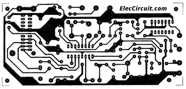
All components, apart from the 12–5 volt converter circuit, can be soldered onto the PCB shown below. Reminding you that components need to be assembled in the intended orientation. Now recheck everything properly, then supply power to the circuit. And make the following adjustments:
Set switch S1 to the second position (100–10,00 Hz), and rotate the VR3 to the middle position. uses an oscillator scope to measure the signal at the positive end of C9. Set S2 to a sine-wave function and rotate VR5 to the middle position as well.
And then adjusting the VR4 until the oscillator scope reads out the best waveform. then go back to adjust the VR5 again, make sure that there isn’t any “clipping” effect, and adjust it again to see if it is actually the best possible waveform.
Rotate the VR2 clockwise and adjust the VR1 until the output signal is 1 volt RMS. As for the square wave, there isn’t anything to worry about.
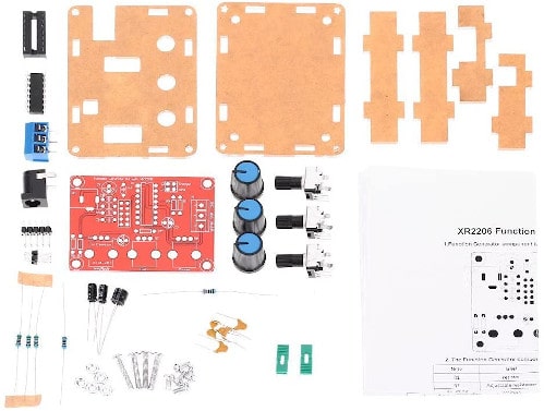
XR2206 High Precision Function Signal Generator DIY Kit Sine/Triangle/Square Output 1Hz-1MHz Adjustable Frequency Amplitude, 10V-26V, temp 0C to 70C: Buy it HERE
Keep reading: Function generator circuit using ICL8038’ »
GET UPDATE VIA EMAIL
I always try to make Electronics Learning Easy.

I love electronics. I have been learning about them through creating simple electronic circuits or small projects. And now I am also having my children do the same. Nevertheless, I hope you found the experiences we shared on this site useful and fulfilling.

plz send pdf file of funcation generataor using xr2206
plz I need typon in pdf
Does XR2206 replace by ICL8038?
sir, i made this circuit ,but it not giving perfect outputs …,
sometimes
1) The xr2206 Ic is heating up
2)Transistor is failing at the sine output
can u help me out from this problem
THANK YOU
sir, i made this circuit ,but isnt giving perfect outputs …,
sometimes
1) The xr2206 Ic is heating up
2)Transistor is failing at the sine output
can u help me out from this problem
Don’t know for sure how to operate it. Please help asap
tank you for this post
it helped me to have my own function generator
Hello Alireza,
It’s okay with pleasure. My compilation of the circuit is useful for you. May the designers of these circuits get good results too.
change your LM7812 12V Regulator for LM7909 9V Regulator
Sory LM7809 Regulator
Hi,
Thank you for your question. We’re glad you’re interested in this circuit.
But we’re sorry we haven’t tested it yet so we can’t fully answer it.
We check this IC (XR2206) , it only accepts a minimum voltage of 10 volts, so it won’t work with 9 volts (LM7809).
In the very near future we will experiment with this circuit.If it works, we’ll let you know via email.
Thank you for following. 🙂