Complementary Transistor RC Oscillator – Sine-Wave or Square-Wave Output

Transistor-based RC phase-shift oscillators are a basic way to generate a sine wave without using inductors or OP-AMPs. In this article, we build and test a complementary transistor RC phase-shift oscillator that uses only two capacitors in its phase-shift network. 

The circuit builds around a complementary pair of old-school transistors: the BC549 and BC556. Apart from sine, it can also be reconfigured to output a square-wave or even pulse signal. At the end, we’ll examine adjusting duty-cycles, amplitude stability, how the frequency equation holds up in real hardware, and more.

Where this Circuit Came From

Before we start, let’s set the pretext; you can skip over to the next section if you please. Recently, we published an article on generating a sine-wave signal using a traditional RC phase-shift network and a transistor, where we also went into the Barkhausen stability criterion. And while working on that, we came across a circuit in an old electronics magazine that claimed to generate a sine signal.

We were interested, of course, so we tried to build a real circuit of the diagram. The result was underwhelming; the circuit does not oscillate as claimed in the book.

Afterward, we tried to fiddle with the component values and placements to get it to work. We also found that the circuit is a different topology of RC phase-shift oscillator, unlike the one we were working on at the time, which helps us better understand it. After all that, we’ve arrived at the main circuit in this article (we’ll take a look at it shortly). This slightly tweaked circuit works nicely as an RC oscillator. It can produce a reasonably stable and predictable sine wave.

With some minor adjustments, we could get it to produce a square-wave or pulse signal as well. Plus, like the aforementioned RC oscillators, this circuit also uses transistors instead of an OP-AMP, making it an excellent progression from our basic circuit. Without further ado, let’s look at this transistor RC oscillator circuit.

1kHz Sine-Wave Transistor RC Oscillator Circuit

With these component configurations, the transistor RC oscillator circuit produces a roughly 1kHz sine-wave signal using two BJT transistors and a few other components. It also seems more sophisticated than a basic transistor RC phase-shift oscillator. But first, let’s see that each component does.

1kHz sine-wave transistor RC oscillator circuit schematic
Schematic of the 1kHz sine-wave transistor RC oscillator circuit.

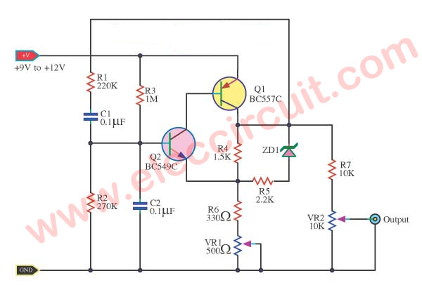
R1, R2, C1, and C2 together form the frequency-selective RC feedback network that sets the oscillation frequency. While R1 and C1 are the main factors in the time constant, R2 and C2 also affect the phase shift and network loading, and changing any of these values affects the oscillation frequency.

The two BJT transistors, BC549 (Q1) and BC556 (Q2), operate together as a single inverting amplifier, providing the required loop gain and 180° phase inversion for sustained oscillation. The complementary nature of the transistors further increases the effective gain compared to a basic single-transistor stage.

R2 connects to ground and provides an AC return path for both C1 and C2, allowing the capacitors to charge and discharge. Although it also affects the oscillation frequency, it is treated here as approximately equal to R1 for simplicity.

VR1 and R3 set the bias current and gain of Q1, while VR2 and R5 influence the overall gain of the complementary transistor pair. Both VR1 and VR2 have a strong effect on startup behavior and the final waveform shape.

R6 and ZD1 provide a form of amplitude limiting by preventing excessive signal swing and reducing clipping after the oscillation has stabilized. R7 and VR3 are for adjusting the output signal amplitude.

Finally, C3 and C4 act as supply decoupling and filtering capacitors, helping to reduce noise and improve waveform stability.

The circuit may look complicated since there are quite a number of components, especially those potentiometers and resistors. They are mainly for adjusting and tuning; we’ll definitely need them, as fine-tunings are usually required when working with transistor circuits.

Of course, we can test and adjust the circuit as we like, then measure the pot resistances and replace them, along with the safeguard resistors, with a single resistor later.

Note: With C2 removed, this circuit can output a square-wave signal. The waveform isn’t perfect since it’s not the intended usage for this circuit, but it’s still a nice-to-have function nonetheless. We learn of this capability while testing on a real circuit, and if you want to know more about this function, how it works, and square-waveform shaping, check out our extended note at the end of this article.

How it Works

Next, let’s try to understand how this circuit operates in practice. From the outset, it is difficult to directly measure the AC currents flowing throughout the circuit, as we currently have access to only a single small oscilloscope.

As a result, the explanation below is an educated guess based on the observed waveforms, bias conditions, and how the components interact electrically. To keep things simple, we’d also temporarily remove unnecessary components from the schematic, leaving only the essential parts involved in oscillation.

simplified complementary transistor rc oscillator circuit schematic
A simplified schematic of the 1kHz sine-wave transistor RC oscillator circuit showing only parts involved in the oscillation.
  1. The moment power is applied, small noise and bias currents appear in the circuit. Through R3, C2 begins to charge, and a bias voltage develops, setting the initial starting point of the RC feedback network.
  2. As the voltage at C2 rises, the base voltage of Q1 also increases slightly, biasing the transistor base-emitter and causing it to begin conducting current via its collector-emitter.
  3. Once Q1 conducts currents, a corresponding bias current is supplied to the base-emitter junction of Q2, activating the PNP transistor and allowing it to conduct current from the supply.
  4. As Q2 conducts currents, some flows through R1 and into C1. This produces a feedback voltage that is returned to the RC network input. At this point, the rising voltage corresponds to the positive half-cycle of the sine wave.
  5. While C1 is charging, C2 simultaneously begins to discharge through R2. The combined charging and discharging of C1 and C2 produces a gradual phase shift rather than a sudden transition.
  6. As the voltage across C2 falls, the base voltage of Q1 decreases, reducing its collector-emitter current.
  7. The reduction in Q1 current also causes Q2 to conduct less current, since Q1 provides the bias drive for Q2. As a result, the output voltage begins to decrease smoothly, forming the negative half-cycle of the sine wave.
  8. With Q2 conducting less current, the feedback into C1 reduces. C1 then discharges through R4 and R5, completing the cycle and preparing the conditions for the next rising half-cycle.

Keep in mind that these steps describe one snapshot of the operation cycle. In practice, these processes occur continuously and may overlap in time.

In summary, this oscillator generates a sine wave through the repeated charging and discharging of C1 and C2, with R1 and R2 setting the timing and phase shift. Transistors Q1 and Q2 act together as one amplifier unit, sustaining oscillation by feeding the signal back in phase with the RC network.

Equation for Output Frequency

Finding the output frequency for this circuit is simple; it’s basically the RC cutoff frequency formula.

$$f=\frac{1}{2 \pi \text{R} \text{C}}$$

Where R = R1 (assuming that R2 is approximately equal to R1), and C = C1 = C2. For example, applying the values we used in the schematic gives us.

$$\frac{1}{2 \pi \times 15.9\text{k}\Omega \times 0.01 \mu \text{F}} \approx 1000\text{Hz}$$

The result at about 1000Hz (1kHz) is in line with the measurement we got from the real circuit later, although we do have to adjust the pots a bit to achieve a perfect match waveform-wise.

Often, when designing an oscillator circuit, we already have a target frequency in mind. In that case, switching f and R around is a more relevant formula. Where f is the known target frequency, and we want to solve for R.

$$\text{R}=\frac{1}{2 \pi f \text{C}}$$

Real-World Test of the Circuit

Apart from the sine, we also tested this circuit in the square and pulse configurations. Below are a couple of images from the experiment.

1khz sine oscillator circuit tested on copper plate to minimize noises
A real oscillator circuit was tested on a copper plate to minimize interference noise.
oscilloscope reading of square-wave output of RC oscillator
An oscilloscope reading of the square-wave output of the RC oscillator.

Want to learn more?

We’ve extended this article on Patreon (19 pages, 2972 words) with extra content, including adapting the circuit to output square-wave and pulse signals, more real-world experiment notes and waveform measurements, a detailed component list, and further proof of the frequency formula.

👉 Read the extended complementary transistor RC phase-shift oscillator article on Patreon

Exclusive posts on Patreon come free of advertisements and in PDF format with high-definition illustrations. Membership fees will allow us to continue to do what we do without as much reliance on advertisement. Thank you very much.

📘 Get Ebook: Simple Electronics VOL.5

2 thoughts on “Complementary Transistor RC Oscillator – Sine-Wave or Square-Wave Output”

    • Hi, in the text he indicates that the Zener is to limit the output voltage.
      Therefore you chose which zener to use, and the voltage of the Zener will be the output voltage.

      Reply

Leave a Comment

This site uses Akismet to reduce spam. Learn how your comment data is processed.