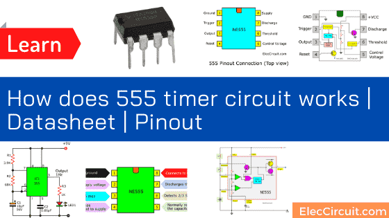
Have you ever used the NE555 timer? The 555 (read “triple five”) is a short way of saying LM555 or SE555 or NE555. I have used it for 36 years. Now, it still is not out of date. Why would we keep using it? Let me explain how to use it in a simple way.
555 timer datasheet
Description
The NE555 is one of the handiest chips to be invented and specially designed to operate as a multivibrator. They can give off time from microseconds to several hours.
It is a TTL device. Thus, it is not sensitive to static electricity. But its power consumption is more than a CMOS chip. Therefore, we must especially attend to this point, when designing for battery operation.
The NE555 takes 10mA from the supply when the output is “high”, and 1mA when the output is “low”. When operating as an oscillator, we can consider the power consumed to be equal to that of an LED.
A CMOS version has been introduced with part number LM7555. But it is considerably more expensive. When the price falls it will be a very good choice as it consumes only 120uA.
Features of NE555
- Can accurate time delays or oscillation
- Timing from microseconds through hours
- Operates in both astable and monostable modes
- Adjustable duty cycle
- VCC—the supply voltage: 4.5V to 16V
- Can output up to 200 mA of current (IO)
- The oscillator does not change frequency even VCC changes.
- Vi—the input voltages(all): VCC
- Output to TTL is compatible. Such as, with a 5V supply, the output is compatible with TTL inputs.
- TA—Operating free-air temperature: 0 – 70C
- Temperature stability is better than 0.005% per ˚C
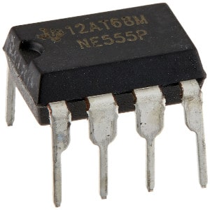
- Available in an 8-pin DIP package
555 timer applications
- Pulse generation
- Time delay generation
- Sequential timing
- Precision timing
- Pulse width modulation
- Pulse position modulation
- Linear ramp generator
Read related: AC dimmer for LED Bulbs using IC-555
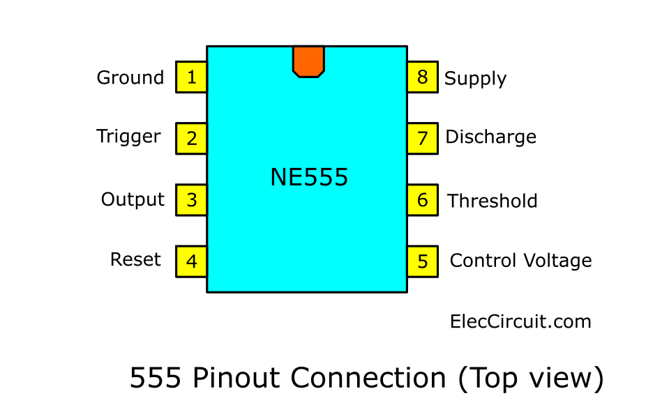
555 pinout
The 555 timers are contained in a tiny 8-pin Dual-In-Line package that looks like a 741 op-amp or LM386 audio amplifier.
Look at its pinout below.
Also: 555 Siren sound Generator
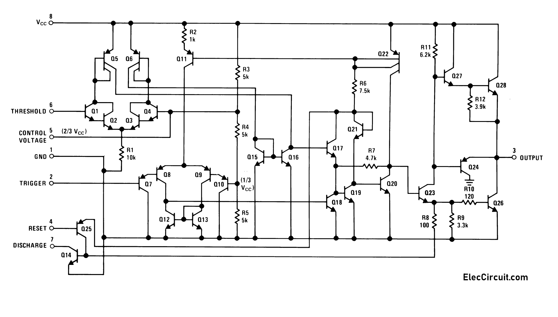
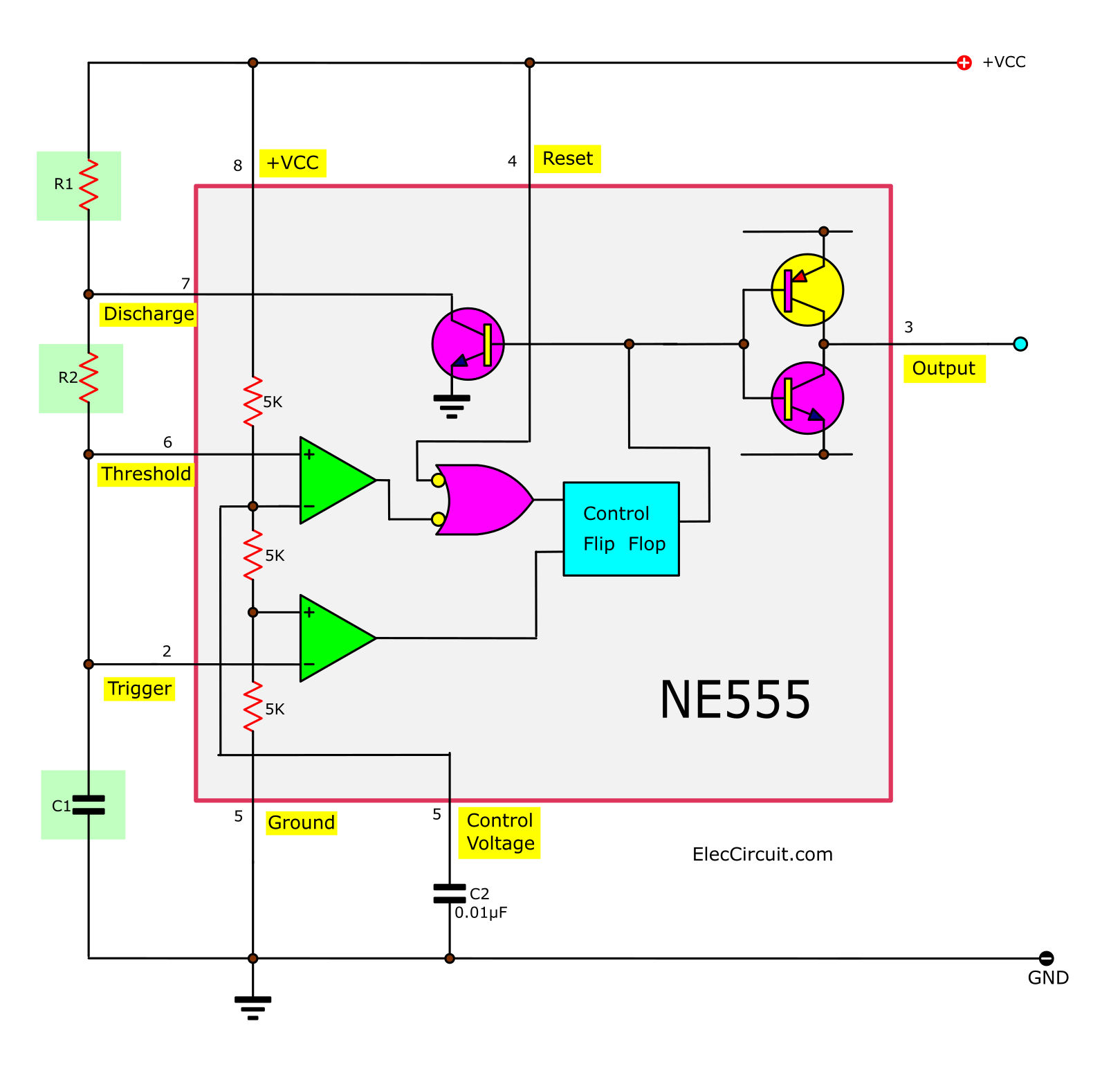
Full 555 schematic
Look at the circuit diagram. This full schematic diagram is mainly to show its complexity. Obviously, it would not be worthwhile to make this circuit from the normal components.
555 Block diagram
The schematic is somewhat simplified, block diagram making the operation of the circuit slightly easier to understand.
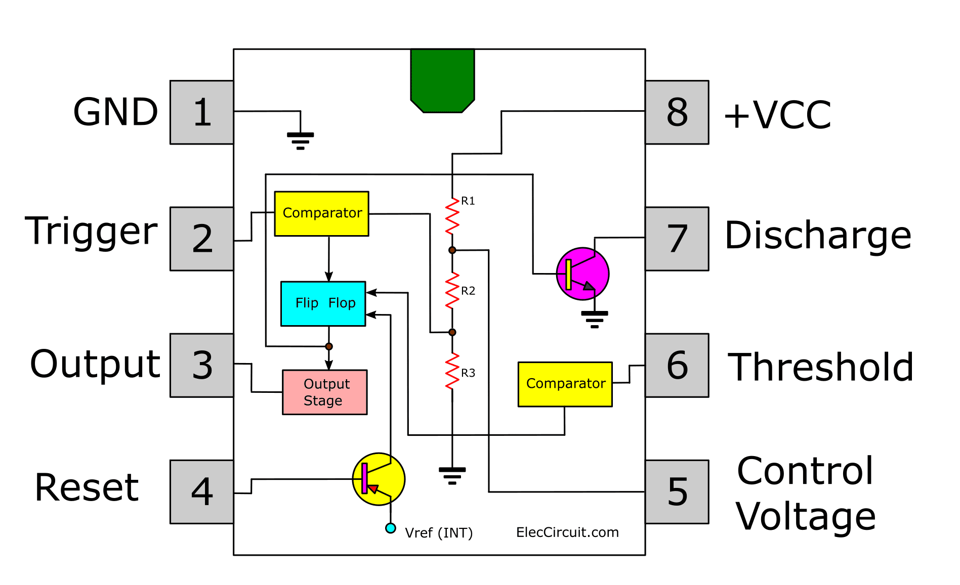
In this diagram, you can see a free-running Flip-Flop which is triggered via pin 2(Trigger) to the comparator and pin 6 to the comparator. Then, drive the Output stage to pin 3 output.
Remember 555 pin Functions in short
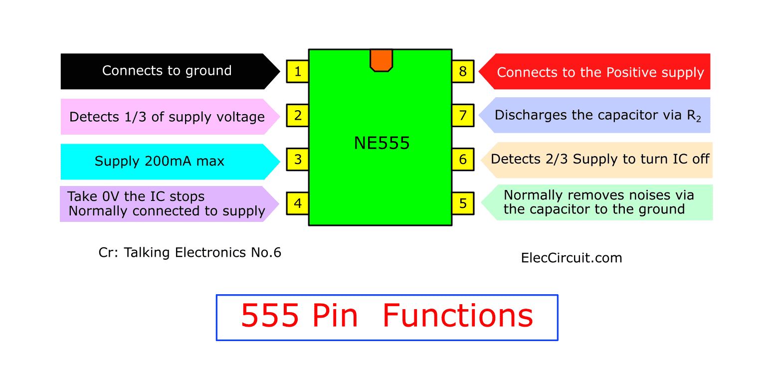
- Pin 1-Ground. We connect it to the 0V rail.
- Pin 2-Trigger. It will detect the 1/3 of the supply voltage. It makes the output turns on. While the pin 2 LOW, this pin has a very high impedance (about 10M) and will trigger about 1uA.
- Pin 3 OUTPUT. If it is HIGH (about the supply voltage) and deliver up to 200mA. In contrast, LOW is about 0.5V above 0V.
- Pin 4 RESET. In normal connect HIGH to turn on IC. Maybe internally connected HIGH via 100K Resistor. It must be taken below 0.6v to reset the chip.
- Pin 5 CONTROL VOLTAGE. Normally we often see this pin connect to the ground via 0.01uF to 0.1uF capacitor. The capacitor to this pin removes external noise.
Also, the voltage applied to this pin will vary the timing of the RC network (quite considerably). We can adjust frequency via an external pot. - Pin 6 THRESHOLD. It detects 2/3 of the supply voltage to turn IC off, make output LOW only if pin 2 is HIGH. This pin has a very high impedance (about 10M) and will trigger about 1uA.
- Pin 7 DISCHARGE. It will go LOW when pin 6 detects 2/3 the supply voltage. But pin 2 must be HIGH.
If pin 2 is “HIGH”, pin 6 can be HIGH or LOW. And pin 7 remains LOW.
Then, the pin 7 will go OPEN (HIGH) and stays HIGH when pin 2 detects 1/3 supply voltage. - Pin 8 +VCC. Connects to the positive rail supply.
How to use 555 timer
There are a lot of ways to use the 555 IC. We can use them in hundreds of different circuits to create many clever things. But they can all be put into three groups. In different types of oscillators:
- Astable Multivibrator – constantly oscillates
– Any circuit which has cycled more than a few times per second like frequencies above 1 cycle per second, is called an oscillator (multivibrator or square wave oscillator).
– Below this frequency, we call it “cycling”. The frequency of oscillation is measured in cycles per second(cps) now called Hertz(Hz). - Monostable – changes state only once per trigger pulse – also called a ONE-SHOT or It is called a TIMER or DELAY.
The 555 timers can provide time delays ranging from several minutes for one cycle of operation to many thousands of cycles per second. - Voltage Controlled Oscillator – called a VCO.
Read next: Monostable multivibrator using 555 timer
How does the 555 timer work
You may not be able to see a clear picture of the 555 timer runs. The standard 555 circuit that we often use is Astable Multivibrator mode. Therefore, we should learn it before.
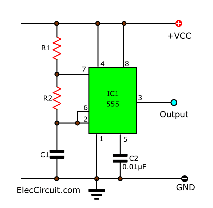
IC 555 timer circuit diagram
When we draw a circuit diagram, always draw the 555 as a building block, as shown below with the pins in the following locations. This will help you instantly recognize the function of each pin:
Look at the block diagram again. I hope you more understand. Credit: Colin Mitchel.
In short, the 555 timer chip works by detecting threshold voltage levels.
- Pin 2 detects a voltage below 1/3 of the supply voltage to turn the IC on.
- And, pin 6 detects a voltage above 2/3 of the supply voltage to turn the IC off.
I’m a student with a slow brain, learning with illustration causes me more understanding. And you? Let’s learn with a block diagram.
- When we connect the IC to the supply, the capacitor C1 begins to charge through R1 and R2.
- Inside the IC, the current flows through the three 5K resistors, and comparator #1 and #2 do their function.
- Then, the capacitor voltage rises to 2/3 of the supply voltage, and pin 6 (Threshold) detects this level and turns the IC off by working of the control Flip-Flop.
- At the same time, pin 7 (discharge) connects to the ground through the transistor circuit inside the IC.
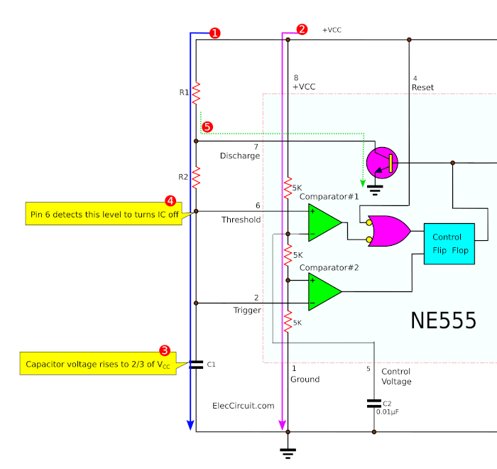
So, the capacitor begins to discharge via R2. Until its voltage is 1/3 of the supply. And, pin 2 detects this and turns the IC on again.
Also, the R1 prevents pin 7 damage. When it shorts to 0v. when pin 6 detects 2/3 rail voltage.
Its resistance is small compared to R2 and does not come into the timing of the oscillator.
In contrast, it does not connect pin 7 to the ground. So the capacitor C1 can charge up again. During this charging period, Pin 2 has no effect, it is disconnected.
Recommended: Simple 555 Timer circuit
Basic 555 oscillator circuit calculator
The 555 output is suitable for driving loads such as relays and LEDs without the need for a buffer transistor.
In the astable (or free-running) mode as shown in the circuit diagram. The 555 triggers itself and the timing capacitor charges through R1 and R2 and discharges through R2 only.
How do you calculate a 555 timer?
Look at the basic oscillator circuit, 1Hz at 50% duty cycle.
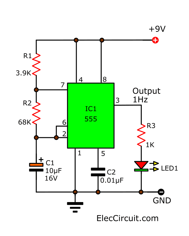
Set duty cycle
We can adjust both resistors, R1 and R2 to set the duty cycle precisely. It can be calculated from:
D = R2 ÷ (R1 + 2R2)
Setting:
R1: 3.9K and R2: 68K
Putting R values into the formula.
D = 68,000 / (3900+136,000)
D = 50% (approx)
In this formula, you can see the top resistor R1 has such a low value with respect to R2 that it has very little effect on the duty cycle.
Find frequency output
The frequency of oscillation of the 555 timers follows this formula:
F = 1.44 ÷ (R1 + 2R2)C1
Setting
R1 = 3.9K , R2 = 68K , C1 = 10 uF
If we take the values for the slow clock rate and insert them into the formula:
F= 1.44/(3900 + 136,000)10×10-6
= 1HZ (approx)
It is easier if you use NE555 Astable Circuit Calculator
Monostable or One-shot Operation
People know it as the 555 timer IC. We can use the 555 as a timer for up to 10 minutes. This circuit is also called a DELAY.
It works in the form of a Monostable or One-shot Operation.
NE555 Example Circuits
Learning by doing is the best. Let’s build these circuits
- 555 Sound effect generator circuit
- 5 circuits of 555 Alarm sound and tone generator
- 555 PWM LED dimmer circuit diagram
Basic dark activated LED circuit using 555
Learn reset pin, if we do not connect the reset pin. It will run because the internal circuit puts a “High” (950mV) on the pin.
But the Reset Pin is more complex:
- Again, No connecting of Pin 4, it has a voltage of about 950mV on it. It will deliver about 350uA.
- Must be below 500mV to turn the chip off.
Then, connect pin 4 to the GND with the resistor
A 2.7K resistor will turn the 555 off.
A 3.3K resistor will turn the 555 on.
This means pin 4 is generating a voltage (and current). So, we can use this feature to turn the 555 OFF using a Light Dependent Resistor (LDR).
Look at the Basic dark activated LED circuit using 555
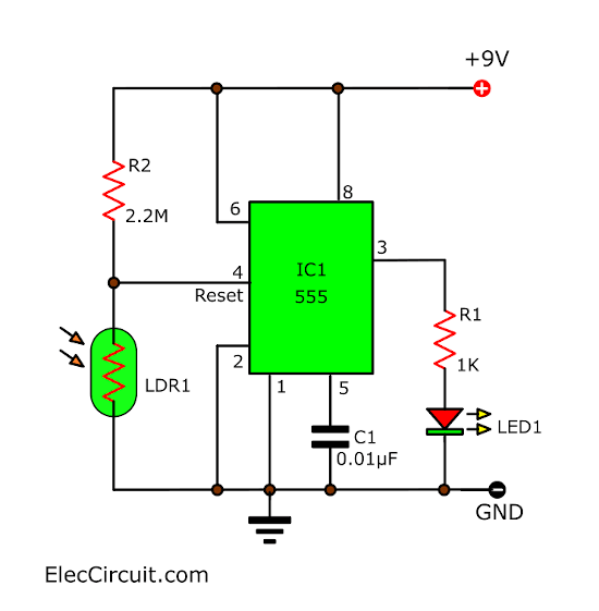
If we connect an LDR to pin 4. It will require a very bright light to reduce the resistance of the LDR to less than 3.3K.
By adding a 10K to the circuit, we help the LDR produce a combined resistance of less than 3.3K. And the circuit will work in a Living room or bedroom.
When the LDR sees illumination from a room light, it will turn the chip off.
You can try values as low as 4.7K to make the chip more sensitive.
In the above circuit, both pin 2 and pin 6 activate the chip to make the output HIGH and LOW at the same time.
But Pin 2 has control over pin 6 and pin 2 makes pin 3 (the output pin) HIGH, too.
Simple NE555 IC Tester Circuit Diagram
Most IC-555 is used to generate frequency, and sometimes we need to know. Is it good or bad? But a normal multimeter cannot check it. Thus, I make a simple 555 ICs tester circuit. Which is tested correctly and faster.
How it works
Resistors R1-R3 acts as limit current and reduce the voltage to LED1-LED3. Which are LEDs show state on “Trigger” or “Low” or “High”. The Diode D1 is set the voltage to pin 2 less than 1/3 VCC (0.7 volts). When slide switch S1 at position 2 (Trigger IC).
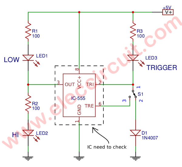
The 555 IC Tester Circuit
Before apply voltage to this circuit, we must put the test IC to socket completely. When entering voltage to the circuit and switch S1at position 3 (no trigger) will see LED1 (low) glow show that the output in state ” low” voltage at the B point about 0.2 volts.
Next, trigger at pin 2 by slide S1 come to position 2 cause voltage at pin 2 about 0.7 volts. Thus the output voltage will change state is “high” voltage at point B about 3.5 volts. The LED2 ( High) and LED3 (Trigger) glow and when switch S1 come to position 3 will cause LED2 and LED3 go out.
In this case, above will show that IC-555 is good. But apply the power supply to this circuit, then switch S1 to position 2. The LED1 will glow but after that slide S1 come to position 3 but LED1 still glow up. If when applying a voltage to this circuit then LED2 will also still grow (S1 at position 2). And slide S1 come to position 3 also still not change state show that this IC-555 bad.
Here are a few related articles you may want to read:
- 20 LED Rear Bike Light Flasher circuit using 555
- Temperature detector circuit with buzzer alarm
- Make Simple 555 Inverter circuit using MOSFET

I love electronics. I have been learning about them through creating simple electronic circuits or small projects. And now I am also having my children do the same. Nevertheless, I hope you found the experiences we shared on this site useful and fulfilling.
Hi Good Day,
A little help, ic 555 called timer?
How can we defeat the timer function?
in other words disabled sleep mode
thanks,
regards & respect
Khairul
thank you
I need help on how to construct a wireless power transfer system using capacitive coupling