Here is the transistor graphic equalizer circuit. Why should make this circuit? We use it for controlling the audio frequency in some kinds of audio frequency responses that are not flat.
Which we cannot use a normal tone control circuit. Because it has a too wide bandwidth.
We need to use a good equalizer circuit that can respond to narrow bandwidth down. And, divide into frequency bands increased to 5 channels or more.
It can control specific actions required by frequency bands.
If you want to learn a basic equalizer. I am going to show you a simple circuit like the transistor tone control circuit.
Read also: TOP 7 Tone control circuit, Low noise
What is more?
How it works
Look at the circuit, without ICs. So, low noise and easy.
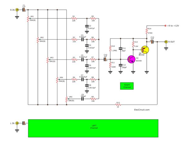
Transistors Graphic equalizer circuit
This equalizer circuit can be adjusted the frequency to 5 channels 60 Hz, 100 Hz, 1 kHz, 3 kHz, and 12 kHz.
And, this project consists of stereos, right and left channels. It is the same. So, we will learn only the right channel (Mono).
In-circuit is Mono. If you want stereo. Just add Mono another one only.
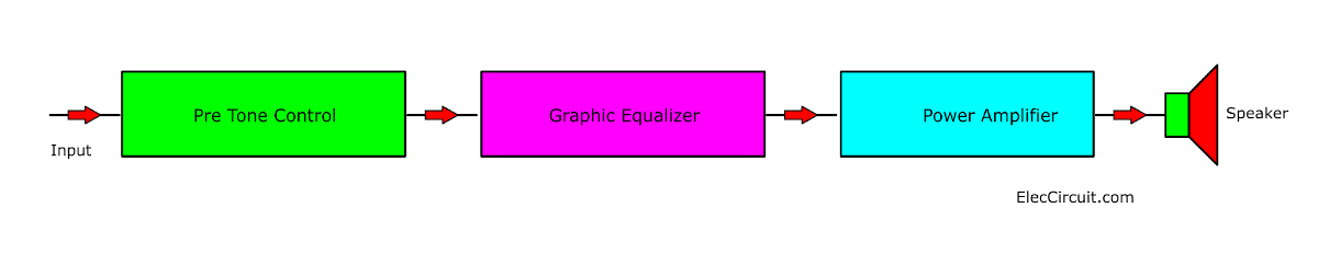
I want you to understand easier. Seeing the block diagram may you more.
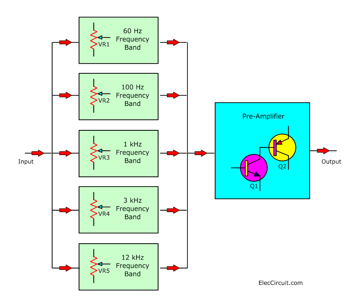
It looks like a preamplifier with a tone control that adds many bandpass filter ranges.
Read next: 4 Preamplifier circuits using transistors
When we enter a signal to the input. Then, C1 passes a signal to coupling through pin1 each potentiometer (VR1-VR5).
If we adjust VR5 to a higher level in the middle of a potentiometer.
This signal will come to a high and low-frequency filter of each band. They include the R and C networks.
Next, the signal that through each band be combined together.
Then, C10-capacitor passes the signal to coupling to a base of Q1 and Q2.
Both transistors are common emitter amplifiers.
The higher signal goes out of a collector of Q1. It is out of phase with the input.
Then, the highest signal or the output signal comes out of the emitter of Q2 via C13.
And, some signals will be feedback through R12 to each leg 3 of the potentiometer (VR1 to VR5).
When we adjust them to this point. A feedback signal will refute with an input. So, this is a cut-off point.
Recommended: Learn transistor circuit works here
How to builds this project
First, find the components of this project. See the parts lists below.
Parts you will need
0.25W Resistors, tolerance: 5%
- R1, R2, R3, R4: 22K
- R5, R6, R7, R8, R9: 33K
- R10: 1.2M
- R11: 220K
- R12: 1K
- R13: 5.6K
- R14: 470 ohms
- VR1-VR5: 50K(B) stereo potentiometer
Capacitors
- C1,C10,C13: 1uF 50V Electrolytic
- C2: 0.047uF 50V Mylar
- C3, C4: 0.022uF 50V Mylar
- C5,C6: 0.0047uF 50V Mylar
- C7, C8: 0.0015uF 50V Mylar
- C9: 390pF 50V Ceramic
- C11: 39pF 50V Ceramic
- C12: 100pF 50V Ceramic
Semiconductors
- Q1: BC549 or BC548 Transistors
- Q2: BC558 or BC557 Transistors
Others
- PCB, Wrres, etc.
Read also: Low Voltage Preamplifier Circuit with Tone Control using transistors
You can see the PCB layout in Figure 2 as Mono.
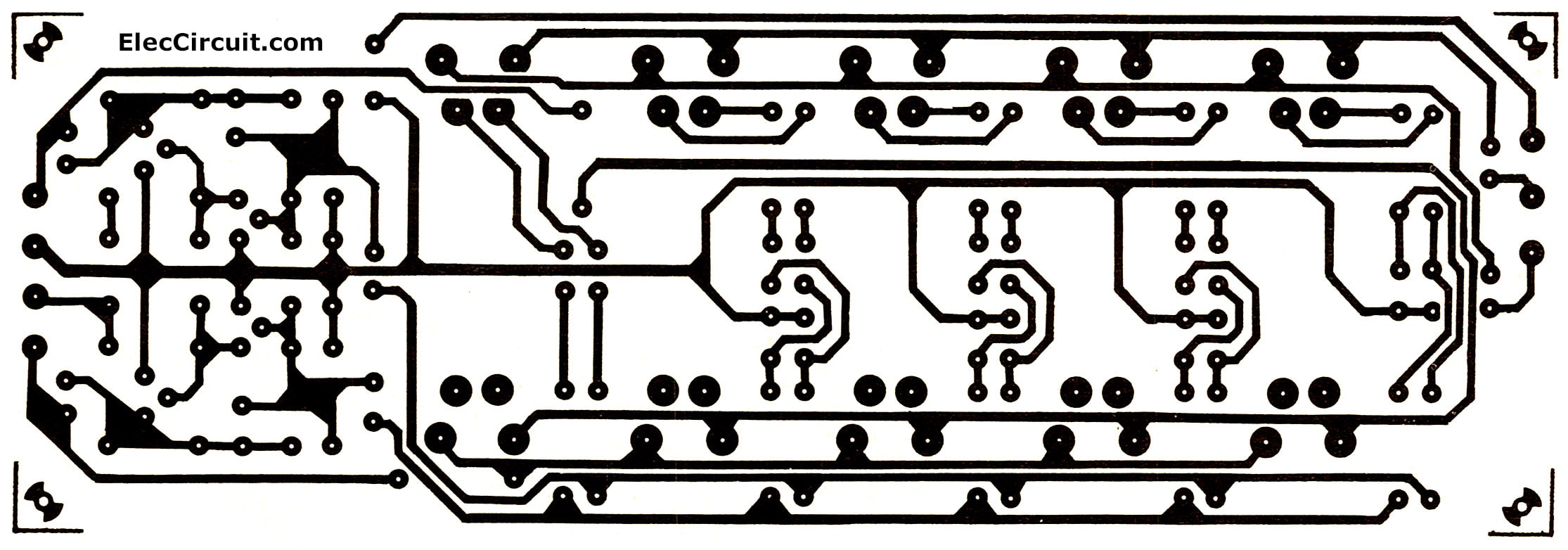
Single-sided PCB layout
And can see the components layout in Figure 3.
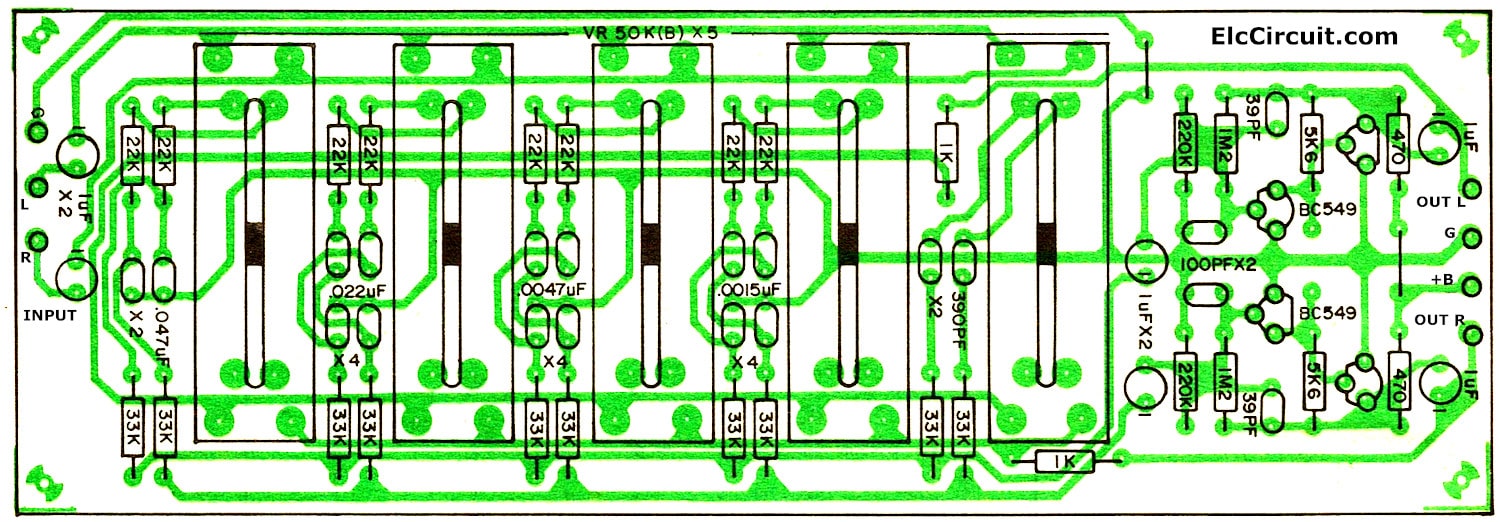
The Component layout of this project in mono.
The wiring for circuit wiring and various parts to check the polarity of the electrolytic capacitors and Diodes and transistors correctly.
Though so easy, you need to solder it with neat.
Note: The PCB layout scale is 200/inch. You can print on the laser printer to make PCB easily.
See Connecting the graphic equalizer to the audio amplifier system below.
Here are a few related posts you may find helpful, too:
- Video amplifier splitter circuit using transistor
- Dynamic Microphone Preamplifier circuit using C945
- Hi Fi audio tone control circuit using low noise transistors

I love electronics. I have been learning about them through creating simple electronic circuits or small projects. And now I am also having my children do the same. Nevertheless, I hope you found the experiences we shared on this site useful and fulfilling.

Your Comment. please I need a project topic for my national diploma certificate
The amplifier part doesn’t work,so I built mine and it’s perfect.
Can i use opamp preamp instead of transistor, after equalizer? I want to use jrc 4558.
I built this project. Good idea, but this does not work. Wasted a lot of time.
Hi Kelly,
I am sorry. It makes you wasted a lot of time.
But I am confident that You develop yourself.
You are who “Look for the opportunity that is hidden in every adversity”.
I was embarrassed. Thanks a lot.
Please recheck it circuit again and
Share your knowledge and experiences.
Great equlazer. It wark fine. Thank you… in components layout ‘in out and out put lines are trap.
Hello Aruna,
Thanks for your feedback. Yes, I just modify the component layout.
Thanks, again
For the equalizer is 60hz channel the 1st or last 50k vr ?
Hello, I’m looking to recreate this circuit but for different frequency channels, can you tell me how you calculated each one? For example, the formula you used to determine that the first frequency channel would be 60Hz using the specified components.
From the experience of this circuit, it can respond to a very wide range of audio frequencies. Because it is Directly coupling, even high frequencies around 600kHz can produce good frequency response. In the case of low frequencies, around 60Hz is possible.
But what you want might be something like this, right?
https://www.eleccircuit.com/high-quality-tri-amplifier-circuits-with-crossover-network-built-in/
Unfortunately I haven’t tried it yet. But in the future, my daughter will definitely try it.
I plan to adapt it for video. Thanks for the starting point.
Dear Apichet Garaipoom:
Could you be so kind to indicate a suitable power supply solution?
My aim is to build your “50W OCL main amplifier using LF351-2N3055-MJ2955”: https://www.eleccircuit.com/the-main-amplifier-50-watt-ocl-by-lf351-2n3055-mj2955-with-pcb/
Although I will try to make it (and this equalizer too) with turret tags instead of PCB.
Could be possible some kind of solution similar to “Power Supply for Audio Amplifier , multiple output 12V, 15V, 35V”: https://www.eleccircuit.com/power-supply-for-audio-amplifier-multiple-output-12v-15v-35v/
The first diagram of this article, if applicable, would be a neat solution.
Thank you.
Dear Quico,
Thank you for your opinion. I apologize if I misunderstood your message from what you intended.
Do you need a suitable (inexpensive and simple) power supply?
https://www.eleccircuit.com/wp-content/uploads/2019/02/50W-main-amplifier-35V-dual-power-supply-circuit-750.png
This is good choice. In the 50W main amplifier has a good power supply circuit with 15V dual regulator circuit within.
It is similar to this circuit https://www.eleccircuit.com/wp-content/uploads/2013/08/38V-Dual-Power-supply-circuit.png, using 7815&7915 Dual regulator circuit. According to my experience My sound quality is sufficient for general use.
For this circuit, If you want the best quality. You may try using a 9V or 12V battery. There will be no noise or humming.
Thanks again.