Have you ever heard about a multivibrator circuit? Perhaps, you may already used it in the transistor circuit form and 555 chip circuit.
Furthermore, we will learn how a Stable multivibrator circuit works when using the digital logic gates.
What is an Astable Multivibrator?
It is a type of oscillator that generates pulse or square signals. It is a simple circuit, which consists of IC, resistors, and capacitors.
How many types of multivibrators are there? There are 2 major types:
- Astable Multivibrator — generated the continuous pulse signals
- Monostable Multivibrator — generated the single pulse signals when receiving external triggers
Biatable Multivibrator
Somebody may say that the RS-Flip Flop is one type of multivibrator too. They call it a bistable multivibrator. It has two stable statuses. If triggered, the status will change. But nowadays we often call these circuits the Flip Flop.
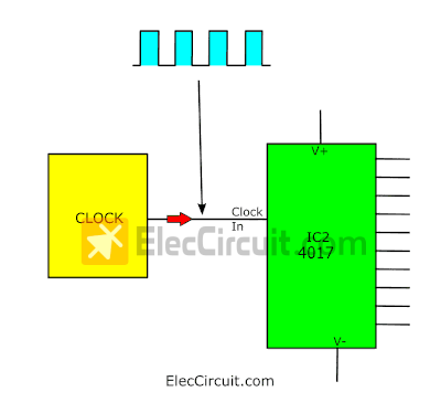
The first type is very popular. Used in the pulse generators, the clock signals. Which use to control the system to run in rhythm, sequence of work, the timing of circuits, etc.
Because the name was too long. We often call it in short Clock.
On the right side is the clock generator to the 4017 counter.
What else? Learn how it works.
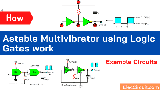
How does Astable Multivibrator work
Look at the simple pulse generator circuit using CMOS Gates.
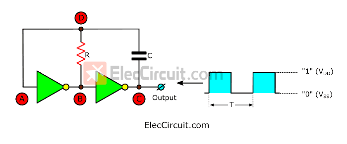
This is a basic circuit of a multivibrator that uses the characteristics of the inverter and the charging/discharging of the capacitor C in the circuit.
Although the circuit looks easy. But it is very challenging to explain it to be easy to understand.
I named the points A, B, C, and D in the circuit, you will see points A and D are connected. But I put them separately for convenience to explain.
The feature of the inverter or Not gate is that the input and output will have the opposite signal all the time.
Here is a step-by-step process.
First, suppose at point C the signal is “1”. Therefore, at B must be “0”.
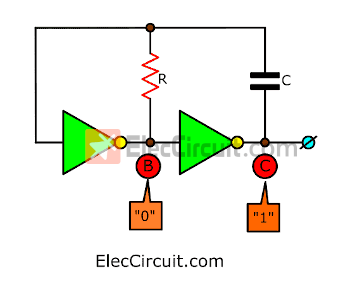
The capacitor charges a high voltage from point C to B. It certainly has the current flowing from C through the capacitor and resistor to point B.
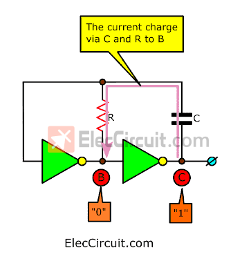
Now, the high voltage is across both ends of the resistor.
It causes points A or D will have high voltage for just a brief moment.
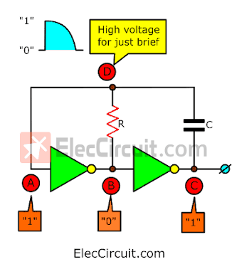
The charging of this capacitor will take less time. It depends on its capacitance and the resistance of R. If the value is large, then it will last longer. But if the value is small, it will last a shorter time.
But when the capacitor is fully charged, the current will stop flowing causing no voltage across the resistor. Therefore, the voltage at point D is equal to “0”.

This was where the change occurred. At the moment, point A is “0”, therefore point B is “1”, and point C is changed to “0”. Every point has the opposite status as its past state.
When point B is “1” and point C is “0”, the current will charge the capacitor again.
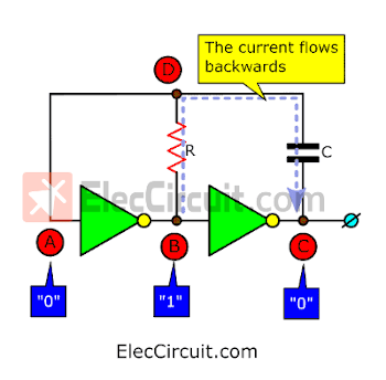
But this time the current will flow from point B through the resistor and capacitor to point C.
Therefore, it has the direction of flow of the currents as opposed to the first charging.
When the current flows in the reverse direction. The voltage across the resistor will have the opposite direction. It causes the voltage at point D to be lower than point B, which point D is “0”.
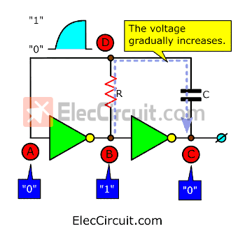
This status will be temporary. Until the capacitor is fully charged. And the current stops flowing.
The voltage at point D gradually increases.
The voltage at point D is as high as point B. As a result, point A is changed to “1”, therefore point B has to be “0” and point C is “1”. Back to the original status as we started to explain before.
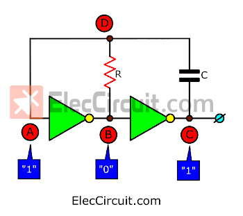
Charging the capacitor and changing of voltage at various parts will continue this way.
See Also:
- Digital Electronics Projects using Flip-Flop Switch Circuit
- NE567 Datasheet Tone decoder/phase-locked loop and example circuits
- Transistor series voltage regulator with overload and short circuit protection
Not only that. if you want to use this circuit. We can design it simpler.
- The resulting waveform will vary with the configuration of R and C in the circuit.
- Try changing the resistor (R) between 10K to 1M and Capacitor (C) between 0.001uF to 0.1uF.
- The frequency of the generated pulse (F) is approximately
F = 1 ÷ 1.4 RC.
You have read this far, have you understood anything? Although, my English is quite bad. But you probably see my efforts, right?
See the example circuits below. They may be useful to you.
Basic clock Circuits
From the above principles, are you bored with it? Let’s see 7 examples of simple circuits
1# Basic 1KHz clock generator circuit using CD4049 NOT Gates
We try to design the circuit to produce a 1KHz frequency. By using the formula above.
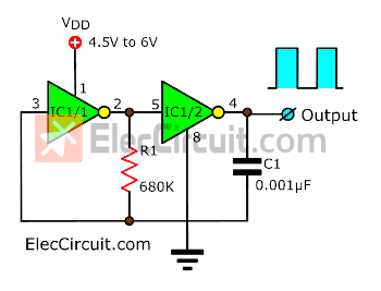
IC1 is CD4049, also you can use other CMOS NOT gates such as CD4049, CD4069, etc. Be careful with a different pinout.
Read: 4049 datasheet and circuits
Read other: astable multivibrator using logic gates
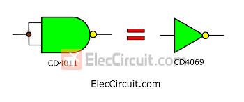
2# 1KHz Oscillator circuit using CD4011 NAND Gates
We know that we can use NOR and NAND Gates are wired as the inverters gates.
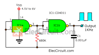
Therefore, we can use a not gate chip for the oscillator too.
3# 1KHz Square wave generator circuit using CD4001-NOR Gate
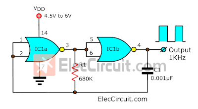
Likewise, we brought the CD4001-NOR gates CMOS chip to generate the 1KHz frequency like the NOT gates.
4# 1KHz Oscillator using Schmitt trigger
We also use a Schmitt trigger to produce a square wave at 1kHz with the components shown on the right side.
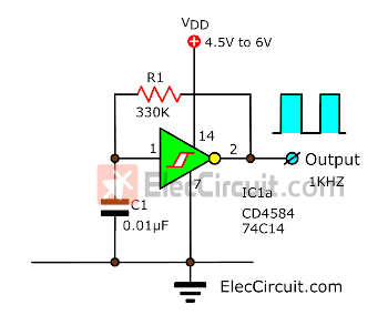
When the Schmitt output is “1”, the capacitor charges via the 330K resistor.
Then, the voltage on the input will rise to the upper trip point of the Schmitt trigger, and the output drops to “0”.
IC1: CD4584 or 74C14 Hex Schmitt Trigger
Next, the capacitor discharges through the resistor to the lower trip point to change the Schmitt output to “1”.
The cycle repeats at approx 1kHz. This circuit is very economical on components.
Imagine you need a high-frequency approx 3MHz. And, you do not have resistors. You may use the below circuit.
5# Simplest High-frequency Oscillator circuit using NOT Gate
Let’s experiment uses NOT Gate as an oscillator circuit. We will try to take an inverter gate or NOT gate to test the fun circuit.
We use the CMOS chip CD4069B inverter gate form.
Or also use NAND gate: CD4011, MC14011B.
Then, take the input joint together into the same inverter form.
Connect the circuit as the figure below. We just to joint pins with many wires onto the breadboard in the correct position only.
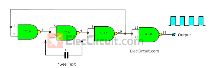
See In the circuit, we connect the inverter ICa to ICd continuously series. The output of IC1c will feedback to the input of IC1a. Thus, the signal will run from ICa to IC1c and backward to IC1a in cycle form.
Then, use an oscilloscope to measure the waveform signal at the output of IC1d. We will see the square waveform signal is high frequency about 3.3 MHz.
Testing without oscilloscope
But if no the oscilloscope, you may test this circuit by applying it near the antenna of the television. We will see that on-screen will have many dots like rain. It indicates the circuit is working with high frequency.
How it works
Why is easy? We use two main principles below.
- The input and output of the inverter will always opposite.
- We enter the signal as the input of each gate. It has a little delay time before appearing at that output.
Here is a step-by-step process.
Look at the circuit diagram again.
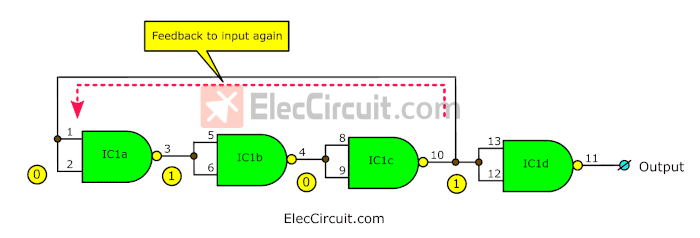
- Suppose that the input of IC1a is “0”, output at pin 3 will is “1”.
- This signal “1” will come to the input of IC1b and provide the output is “0”.
- Then, it changes to “1” at pin 10 of IC1c. After that this signal is sent to feedback to input IC1a again.
Therefore, the input of IC1a will change from “0” into “1” automatically. And it will return back through IC1a to IC1C again. At the same time, this signal “1” will flow through to the input of IC1d to output into “0”, the signal will is “0” and “1” alternately all the time.
Key Tips
Connecting the inverter circuit as the oscillators. We must use the gate as an odd number such as 1, 3, 5…. etc. If even numbers will not cause oscillations.
Also, the frequency of the oscillator depends on the delay time of each gate and the amount of the gate, too.
- CMOS—they will have a delay time of approximately 0.1 uS.
For example, if we use the 3 gates connected as the delay time of 0.3 microseconds. Therefore, the output frequency of 3.3 MHz. - TTL— this type will have a delay time of about 20 nanoseconds. Which is faster than CMOS by 5 times.
For example, if we use the 74LS00 NAND gate. It can get a frequency waveform of approximately 15 MHz.
Reducing Frequency using the capacitor
If you do not want too high-frequency output. How to reduce it.
Suppose that, in the gate circuit, there is something that makes the long delay time up. It will make the frequencies certainly lower.
We connected a little capacitor across the inverter as figure above.
When we insert the capacitor connects between the input and output of IC1b. It will cause the delay time at the IC1b to be longer up. After that, try to measure the waveform. we will see that they have lower frequencies.
We may change the larger capacitances. To find out the result reducing frequency down as table in right side.
| Capacitor | Frequencies |
| NON | 3.3MHz |
| 220pF | 720kHz |
| 0.01uF | 31kHz |
| 0.1uF | 3.2kHz |
Now, probably understand the basics of the Astable Multivibrator circuit using the Digital Logic Gates.
In fact, there is still much more to this section, but I’m afraid that this article will be too long. You may feel bored. What would you most like to learn in the digital world? Why?
Check out these related articles, too:
- 4011 Tone Generator circuit projects
- 5 Crystal oscillator Circuits using CMOS
- Simple VCO using Schmitt trigger using 74HC14
Download This
All full-size images and PDFs of this post are in this Ebook below. Please support me. 🙂
GET UPDATE VIA EMAIL
I always try to make Electronics Learning Easy.
Related Posts


I love electronics. I have been learning about them through creating simple electronic circuits or small projects. And now I am also having my children do the same. Nevertheless, I hope you found the experiences we shared on this site useful and fulfilling.
Seu Inglês pode não ser bom, mas a didática é muito boa. Parabens!
Hello José,
Your message makes me happy. I will try to improve my English continually. I’m very glad to see that, my content is helpful. Thank you very much for the birthday wishes.
Can you please write more correctly? It is more difficolt understand what is written than the circuit itself.
Yes, you can. But during this time, my family is sick with covid. almost two weeks ago when healed will start editing this article.
IN MY OPINION ENGLISH IS VERY UNDERSTANDABLE, BUT IT DOESN’T SEEM VERY KIND TO REMARK IT, CONSIDERING THE EFFORTS MADE BY THE AUTHOR! MOREOVER YOU TOO MADE SOME MISTAKES ON YOUR WRITTEN!
Hello,
As for my English writing, it is undeniably bad—some parts were even considered unreadable. But in the last few months or so, we have been trying our best to improve our writing in our new posts or even rewrite some of our old posts on the website.
But perhaps if you were to be so kind as to give us a piece of advice or two or even point out some of the things that we might have done wrong, that would help us tremendously improve our understanding of English writing even further.
Thanks,
Keep the good work rolling.
But I want to ask as electronic hubbist but who could not get chance or know how to start carry out electronic projects posted on this platform or see somewhere,where to start from?
Thanks.
I very much appreciate your question. It might be a great idea. I and my kids will compile how-to and ideas to create simple electronic projects for hobbyists and beginners. Please be patient.
Great job!!! I fully understand you!!!
Thanks for your feedback.
I designed a 455Khz oscillator gated with a 4011. 1khz generator..great for aligning radios!!!!!!!!
Oh! it is a great idea. I will teach my daughter to learn about AM radios. But now she loves LED flasher and LED running circuit. Never mind, electronics has a lot of information to do (fun).