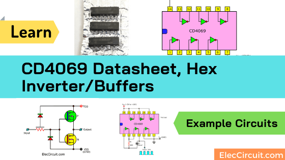
You probably know that the inverter logic gate is very important in digital circuits. We have many ways to do it. But often I use CMOS digital IC. Because it is easy and cheap. CD4069 is one IC that I like to use.
Sure, it will work well. If we know the basic details, pinouts, features. Especially examples circuit diagram. To be a guideline for creating more diverse circuits.
Short Description of CD4069
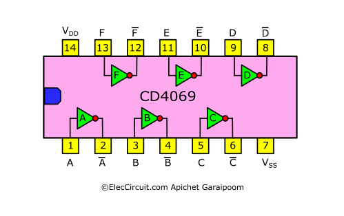
See in Fig below. The CD4069 consists of six inverter gate circuits in 14 DIP packets.
The manufacturer uses CMOS technology, which allows it to use a wide voltage range of 3V to 16V. Imagine, you are using 2 of 1.5V AA batteries. This IC is working. And It uses low power consumption.
Also, it has high noise immunity, and the symmetric controlled rise and fall times.
We can use them for all general inverter applications, medium-power TTL-drive. Or even logic-level-conversion capabilities of circuits. For example the CD4009. And we do not need to use CD4049/MM74C04 hex inverter and buffers.
Recommended: If you are a beginner should read CMOS characteristics before.
CD4069 pinout
See the HD14069 made by Hitachi. They are equivalent to CD4069. And Connection Diagram or its pinout below.
Equivalent CD4069
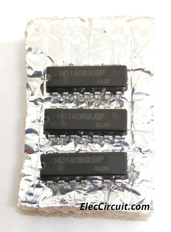
Sometimes you may not be able to buy CD4069. We can use other numbers instead, with the same features, MC14069, TC14069, HD14069, etc.
Buy the CD4069 at Amazon.com here (affiliated link)
Schematic Diagram
Look at the Schematic Diagram of CD4069 inverter gates. We can see that it consists of the structure of MOSFET N and P.
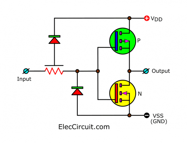
According to the principles of CMOS, it gives us a great inverter gate logic. That uses very low energy And good performance.
But It is a high-impedance input. What is more?
Static discharged protection
Have you ever worried that the CMOS is easily damaged by static electricity? Yes, me too. But when we look at the internal structure of CD4069 above.
All input is protected from damage since the static discharged by diode clamps to VDD and VSS.
Applications
- Logic inversion
- Pulse shaping
- Oscillators
- High-input-impedance amplifiers
Example circuits
You want to use it right?
We learn it by experimenting with creating simple circuits. You can easily assemble these circuits using the breadboard.
1kHZ Clock pulse generator
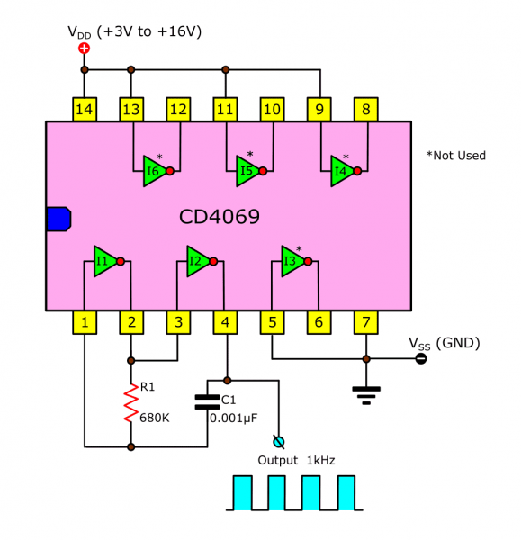
The output is a square wave frequency or pulse form. And F = 1 / 1.4 RC.
Also, you can learn how this circuit works here: How Astable Multivibrator using Logic Gates work
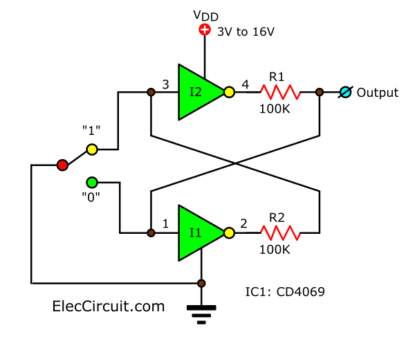
Bounceless Switch circuit using inverter gate
High-Input Impedance Amplifier
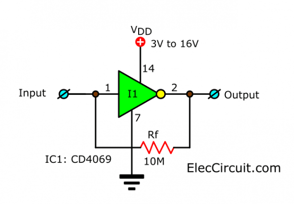
Suppose your input signals are weak. It may make the circuit work error. We need to increase it before a feed to the circuit. The easy way is using an inverter or buffer gate as a high-impedance amplifier.
Later we will see a power amplifier using a digital logic gate.
Remember
Watch out static electricity
It is one type of CMOS Digital IC. So, we should be careful about static electricity.
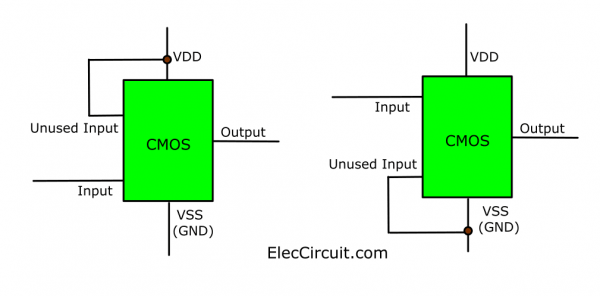
Protect inputs
All Unused input pin should connect to the VDD or VSS(GND). To protect CMOS work mistakes.
Read Also:
- IC 4049 Hex inverter Datasheet – Square wave oscillator
- Cheap Christmas LED flasher circuit is controlled with audio
- 24 LED Decorative light circuit using NOT Gate
GET UPDATE VIA EMAIL
I always try to make Electronics Learning Easy.

I love electronics. I have been learning about them through creating simple electronic circuits or small projects. And now I am also having my children do the same. Nevertheless, I hope you found the experiences we shared on this site useful and fulfilling.