Imagine you are using CD4011. You know that it is a CMOS Digital IC. Of course, you may use this IC without understanding it enough. But, Is it better? If you know it works.
For maximum efficiency, reducing various problems well. Let’s learn the characteristics of and CMOS circuit.
What is a CMOS circuit?
It’s a digital IC with an important element in the MOSFET. We don’t need to know its structure thoroughly. Because you probably don’t think of building it, right?
Currently, the internal structure of both P-MOS and N-MOS is on the same chip for lower power consumption. We call it CMOS (complementary MOS).
This type of digital IC As widespread as TTL (older). Some family the same number as the TTL.
I like to use them, and you?
Why?
Operating Requirements of CMOS
Then, we will look at the important features of CMOS. This is the reason that I love them:
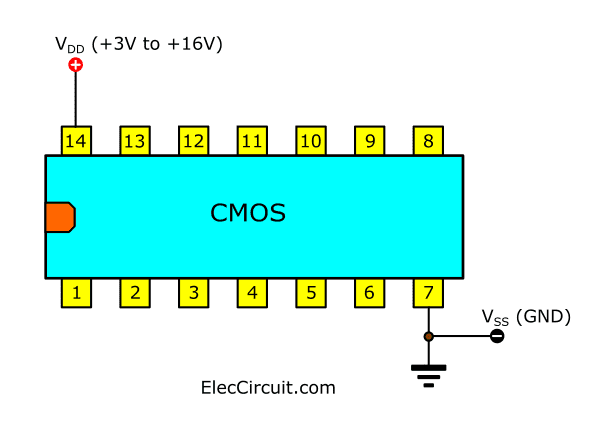
CMOS Power supply
- Requires a wide voltage power supply of 3V to 16V.
Imagine you can use 2×1.5V AA batteries (3 volts). But the efficiency is lower than the voltage level 5V, 9V, or 12V.
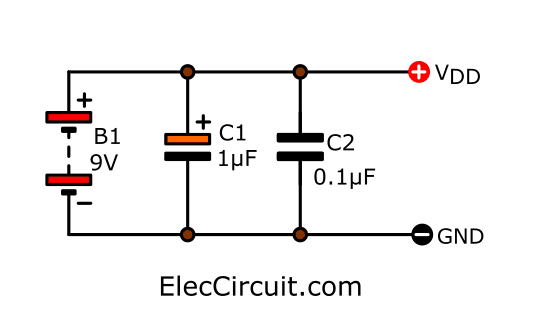
See the power supply for CMOS below.
9V power supply circuit for CMOS
Above the CMOS using an easy power supply. Because it uses lower current and wide voltage range. Look at below
For basic circuits, you can use the 9-volt battery as its power supply.
Important, we need filter both capacitors (C1, C2). They are a transient killer to reduce any noise.
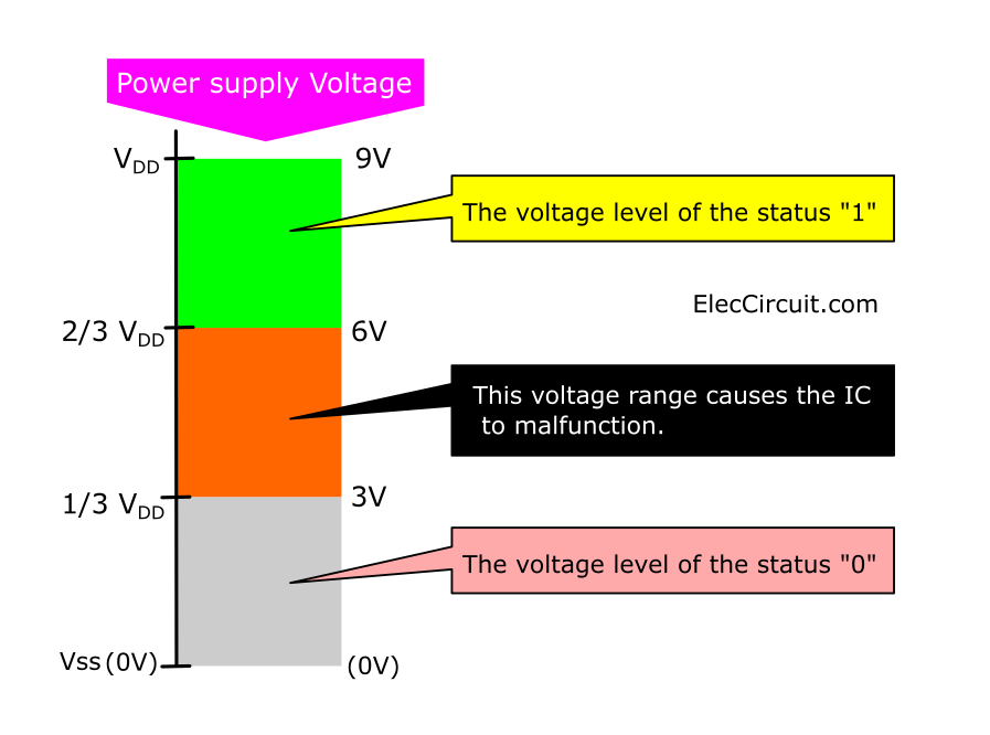
Digital status of CMOS
We know that digital circuits have the status “1” and “0”.
How much voltage level in the CMOS IC?
We usually specify that 2/3 of the power supply voltage level is “1” and 1/3 of the power supply voltage level is “0” status.
See for example We use a 9V battery.
If the voltage level is less than 3V, the status is “0”. On the other hand, the high voltage level is 6V, the status is “1”.
But be careful, the voltage between 3V to 6V may cause IC to malfunction.
Read other: CMOS Technical details
Why should to use CMOS?
- Uses less current than other digital IC.
For example, the basic Gate chip uses the current of 0.1mA only (in standby mode).
Even the wristwatch chip uses a CMOS type IC. We only use a small battery. But can be used for up to 1 year. It consumes electricity almost zero. - Use 74Cxx series it looks like TTL.
For example 74C04, a CMOS that is equivalent to the TTL, 7404. This modern CMOS has a high speed. It has a capability equal to TTL.
Note: If you are a beginner should Learn electronics for beginners
Cautions and advice
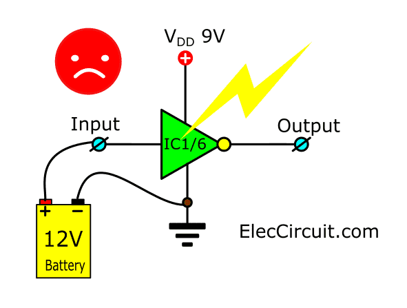
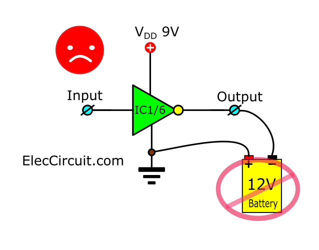
- Must Never enter the power supply to the wrong polarity. Because the IC was broken instantly.
- Avoid entering the input signal that is rising slowly and decreasing slowly. Because it will cause the IC to use too much power.
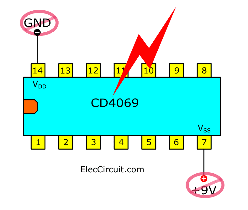
- The unused input pin.
We should always connect them to VDD (V +) or VSS (GND).
Note that unused input grounded (in short).
Look at the right. It is a 1kHz clock oscillator using CD4069.
We do not use the I3 to I6. So, we connect to VDD and VSS.
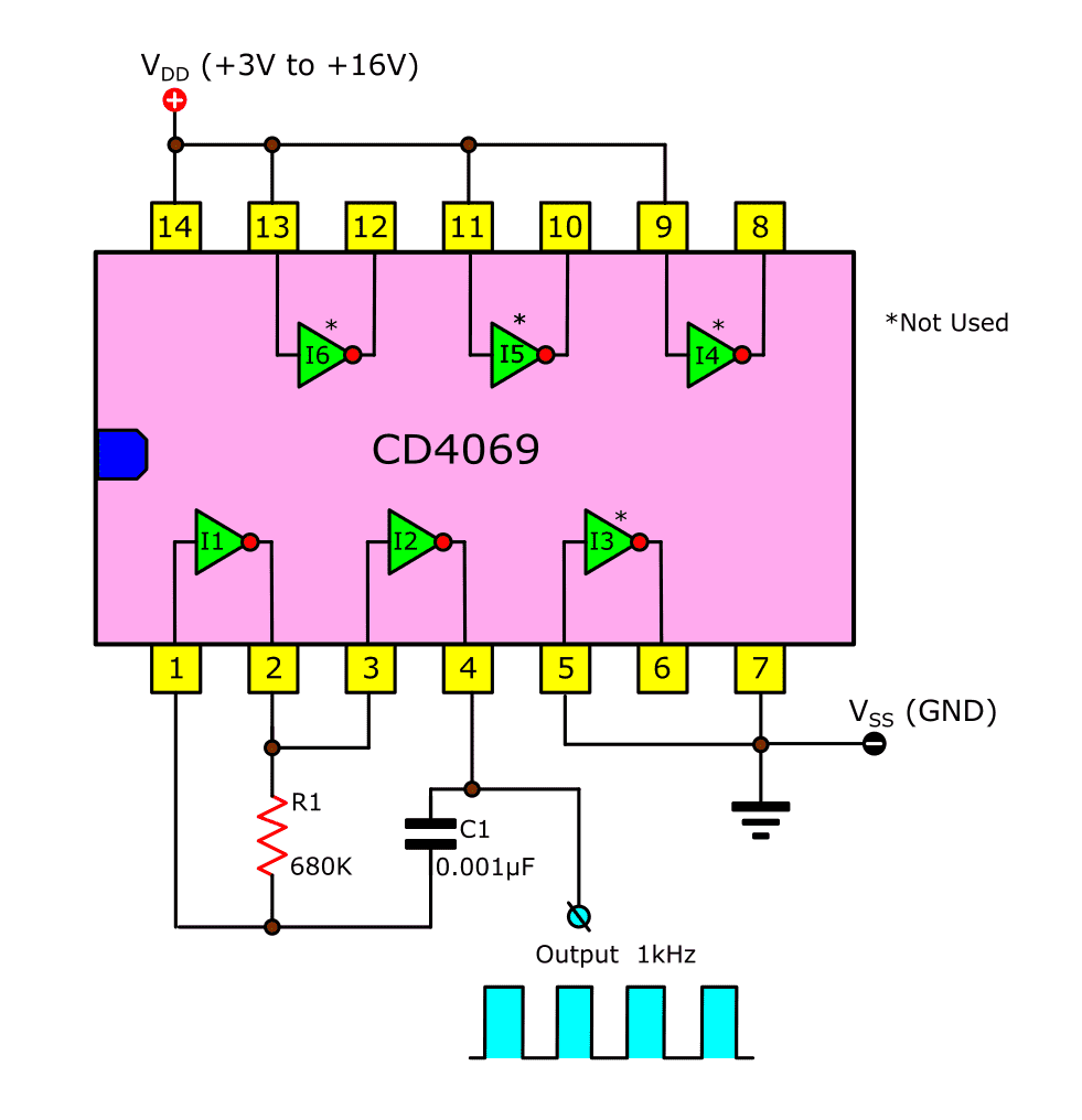
Otherwise, it will cause the IC to malfunction. And consume more power than usual.
Because the CMOS input has a very high resistance, Therefore is sensitive to various interference signals.
Note:
Now, inside of CMOS IC, even the producer inserts the circuit to solve this problem. But we should always be careful about this.
- The input voltage should not exceed VDD(Power Supply voltage). Except for IC numbers CD4049 and CD4050.
- Do not connect the signal to the CMOS IC. Once the power supply has been stopped.
- Every type of IC is afraid of the heat. Do not solder the IC pin directly for more than 10 seconds. If a beginner should use an IC socket better.
- Do not connect the wrong circuit. Such as the output of the IC directly to the power source. It may damage the IC.
Even if the CMOS has a built-in protection circuit. So be careful.
When turning on the power switch or enter the power supply.
We should always check the correct connecting of the circuit, especially the output of the circuit.
- Be careful when handling the IC.
- Should not bend the legs of the IC. It may cause cracks in the internal structure. Then, Make shorten its lifespan.
Anti Static discharge
Another very scary thing for CMOS is electrostatic. It happens easily around us.
The most dangerous leg is the input pin. The resistance of The input pin of this type of IC is usually very high. It has the same properties as insulation.
These input pins may take static electricity from anywhere to store it.

When it accumulated a lot. There is no way to drain it which can damage the circuit at the input area.
Currently, IC production technology has developed a lot. The input side of the IC has a protection circuit inside. It is therefore not easily damaged anymore.
But for not being careless. Prevent unexpected events.
I keep the IC in a metal sheet or foil, conductive foil, or aluminum paper. Then gradually in a plastic bag again
How to use CMOS IC
Now that we’re starting to understand the nature of CMOS. Next, let’s try to find it out and make a circuit. You should know about it first. because sometimes it may help you pay less, but the result is the same.
CMOS Families
In the assembly of electronic circuits. We often use many ICs. Each of them should have the same features. For example, use the same power supply, the signal voltage is equal, etc. When those ICs are connected, Therefore not a problem.
Therefore, the manufacturer so produces ICs in groups with the same electrical properties. We call it the CMOS family.
Examples of different families include:
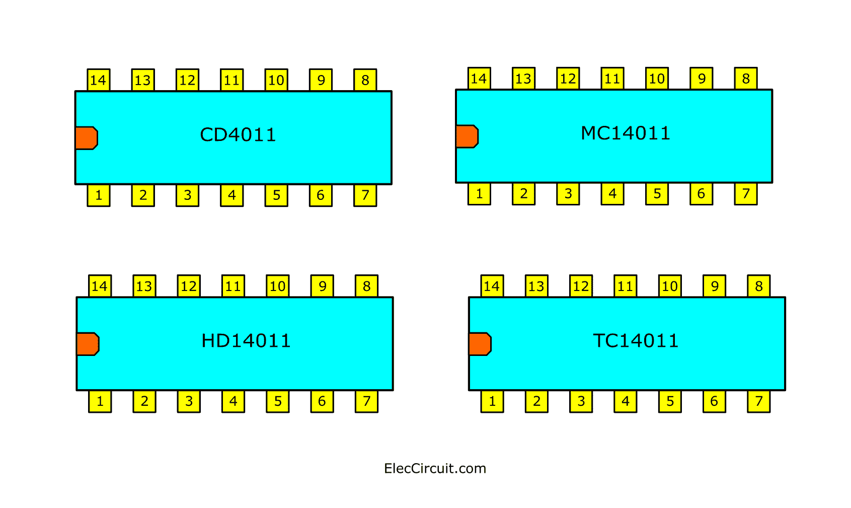
- CD40xx is a CMOS IC with RCA being the first manufacturer.
- The MC140xx family is an IC company from Motorola.
- The HD140xx family is an IC company from Hitachi.
- The TC40Hxx family is a high-speed CMOS IC manufactured by Toshiba.
- etc,
These companies develop and sell copyrights to other companies made out for us to use together. At a decreasing price.
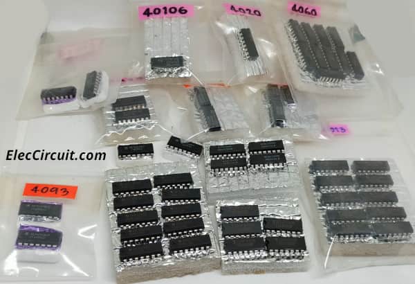
For you to see more pictures Let me give you an example. If you want to use the 4011 NAND GATE. You have many options or numbers. To choose from, with the same leg position and features.
Look at the right: CD4011, MC14011, HD14011, TC14011
CMOS circuit List
- IC 4017/CD4017 Datasheet | Pinout | 15 example circuits
- CD4047 Simple Astable multivibrator Circuit
- 4011 Tone Generator circuit projects
- Simple IF signal generator circuit using CMOS
- Variable Timebase oscillator circuit CMOS
- Sound effect generator circuit using CD4040 CMOS
1# Buffer circuits for digital CMOS
If you want the circuit Output buffer for the circuit digital. I suggest the IC-4050 (Hex buffers with high-to-low level shifter inputs) because very be IC that be usable easily. use link up digital circuit TTL and CMOS well.
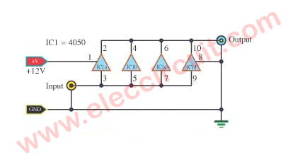
The family of CMOS digital ICs has many strengths. It can be used to power a 3-16V, Easy and cheap. It has the same frequency is not high. A slow response that IC – TTL applications are easy to use and cheap. Slow response to IC – TTL applications. The problem that I found as the current is low. Do not apply to other circuits or the load current is greater than 50mA. However, we have several ways to increase the buffer circuit such as the transistor and a buffer circuit. This circuit continues on this issue, we use the IC 4050 is characterized by several parallel butter gate. However, we have several ways to increase the buffer circuit. Maybe uses a transistor and a buffer IC circuit.
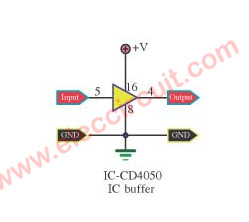
In this circuit, the answer to this problem, we use the IC 4050 is characterized by several parallel butter gate. Normally single gate circuit can supply up to about 15mA. When we put the gate parallel together will help Increases the current very well. The circuit is in highly stable up.
Recommended: How Astable Multivibrator using Logic Gates work | Example Circuits
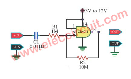
2# Linear x10 Amplifier using 4011 Gate
This is very basic amplifier circuit,so I use IC digital Cmos 4011 quad NAND gate.
It is to give equal to 10x linear amplifier.
The resistor R1 = 1M ohm , R2 = 10M ohm.
This circuit can not output speaker because it is very low power amplifier.
3# 1 Hz Timebase circuit using 4017
I used input frequency 10Hz to output 1Hz. This is a 10 divider circuit.
When we need a standard digital clock of 1 Hz. but we have the input signal is square waveform 10 Hz so need to reduct it lower with digital frequency divider circuit 10 times.
I suggest that IC 4017 (Decade Counter / Divider with 10 Decoded) from the familiar to make 10 LEDs running light circuits, but this circuit we used a frequency dividing circuit 10 times, too.
It’s interesting because it uses a single IC to run it. The circuit is very simple. Would not be very descriptive. Enjoy it.
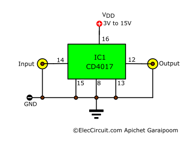
Circuit diagram of the 1 Hz Timebase by IC-4017
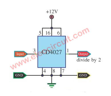
4# Two divide counter circuits using IC-4027
When you want to decrease the frequency in 2 digital times circuits or Divide Frequency by 2 counter. I advises use IC 4017, because seek easy cheapness can be usable good various.
A diode protect CMOS circuit
The CMOS digital circuit used to produce an oscillator, with pulse low-frequency form. We use R and C are a lot of period of time. it must have a diode to prevent current flow feedback.
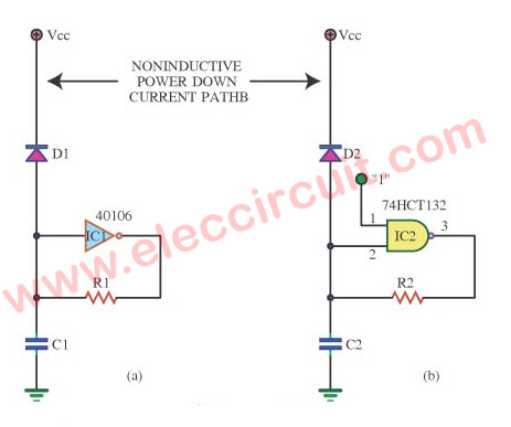
In the oscillator circuit, we use the CD40106 and 74HCT132.The D1 and D2 connected to the input terminal of the twin IC respectively. These diodes should be outside the IC, because if the diode within the IC. When too much current flow will cause the loss diode and IC too.
Level Voltage of Logic Changer using JFET
This is a logic signal changer circuit, the normal voltage of about 5V. But sometimes we want to 12V or 15V, we can use a JFET. It works by mode COMMON GATE.
The simple principle is that when a logic “0” or 0V. The JFET N-channel type which will stop the conduction, The voltage between D and G was 0V too. And if logic “1” with the voltage 5V, N-channel conduction.
The voltage between pins D and G is equal to VS, which may be equal to any 12 Volt or 15 volts.
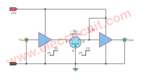
The R1 will determine the speed and power loss of the circuit, the resistance R1 is in the range of 100K to 1M, so the current flowing through it is in the 150uA to 15uA.We can also determine the frequency of the pulse matches with. The limit of approximately 1 MHz.
A key advantage of this circuit is, can be applied to the device driver voltage is higher than 5 volt.
Automatic duty factor controlled circuit
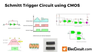
This is an Automatic duty control circuit. We can use the Schmitt trigger to generate the simple square wave. The duty factor of the output waveform will be determined by the input waveform. But the threshold level is the importance.
In Figure 1 will have the output while input waveform as Figure 2 cannot have output.
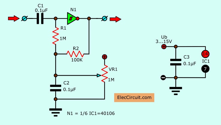
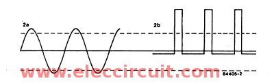
Figure 2 the waveform of this circuit
How Automatic duty control works
The small input signal is connected to the circuit through the capacitors C1. The level of output is the average by R2 / C2 and feedback to input.
The adjustment of the DC voltage at the input to control the peak voltage of the input signal.
When the input signal is fed into a large excess of the threshold level of Schmitt trigger both positive and negative side. It will be a square wave at the output. The sensitivity of the tuned circuit at P1.
The disadvantage of this circuit is that. If no the input signal. The circuit is working as a frequency generator. To prevent this problem, We must have a frequency of at least 10 times. (The circuit is 100 Hz,)
Using this circuit may be used as a trigger to automatically oscillator’s frequency spectrum.
Another disadvantage of the circuit. If the input signal is a very small duty factor at the top of the sign. The pulse output quality is not good.
Parts you will need
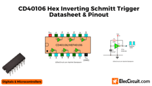
IC1: CD40106, CMOS Hex Schmitt Triggers
R1: 1M, 0.25W Resistors tolerance: 5%
R2: 100K, 0.25W Resistors tolerance: 5%
C1: 100nF or 0.1uF 50V, Polyester Capacitor
P1: 1M Pot
See other simple electronic circuits
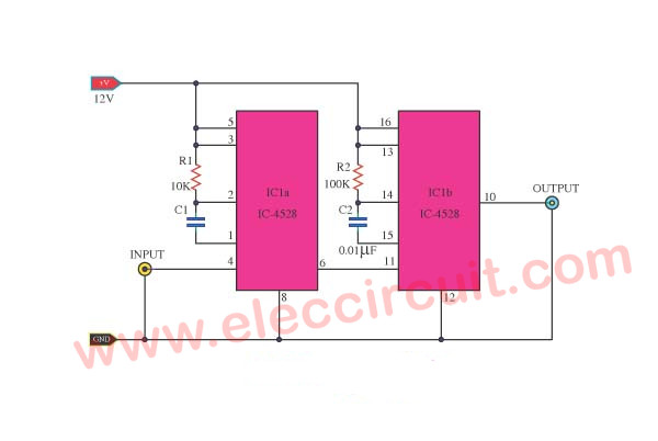
Pulse delayer circuit using CD4528
The Pulse delayer circuit this use IC 4528 help delay pulse or oscillator the all. For a signal is a pulse that postpones long ago go up. By fix give R1 control while delay, R2 control the wideness of pulse to delay. The detail is other see in circuit picture.
7 Stage Binary Counter Display with LED using CD4024
This circuit basically the base of the usability IC number CD4042 (7 Stage binary counter). By the circuit will regard the binary digit arrive at 128 BIT. Then show with LED 7 the make easy build the education.
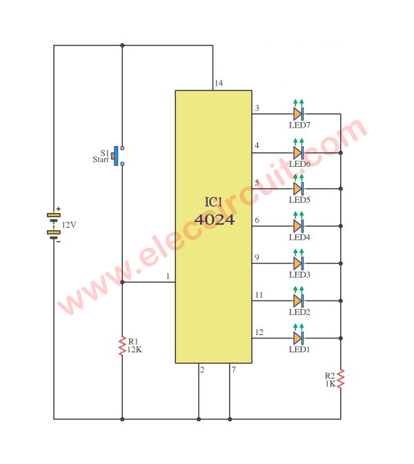
When feed power supply give with the circuit IC1 as a result will change way position output every time. When receive pulse signal from pressure switch S1. By pin 1 (CK) will receive pulse signal pin edge goes up to are logic “1” and when liberate switch receive signal pin edge down is logic “0” thus when press switch S1 time that 2 LED2 stick bright. But LED1 switch off which be the show output the two base is 001 and when press switch S1 time that 3 LED1 and LED2 stick bright. But LED3 switch off display be output the base is two be 011. when press switch time build go to as a result will display be the binary digit goes to continually until arrive in time that 129 which LED1-LED7 will stick bright and the integrated circuit will do something reset begin count at new zero output every a leg has will logic “0” cause LED1-LED7 switch off be finished every.
4511 Binary to Decimal decoder
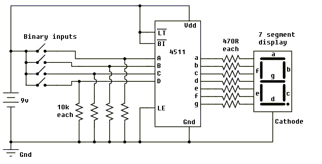
This isn’t a very useful or interesting circuit but it demonstrates the prinicple of a Binary to Decimal decoder IC such as theIC 4511.
Counter Display with LED 7 Segment Using CMOS
This is the simple digital counter circuit, the IC application number 4029 from binary data, and then sent to the IC number 4513, a driver IC 7 Segment, to show off a digital number from 0 to 9.
When entering into a pulse signal input pin 15 of IC1, it will signal to the output signal is Binary.Then send the output from the pin Q0, Q1, Q2, Q3, and the pin. 6, 11, 14 and 2 of IC1.Go to the input of IC2 No. 4513. Which is IC displayed by the decoder signal to the Binary LED display with a 7 or the 7 Segment, will be displayed from a digital number from 0-9.
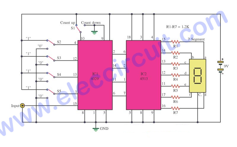
The Schematic Diagram of LED 7 Segment Counter circuit using CMOS
0-99 Two Digit Counter By IC 74LS48 , 74LS90
This is circuit 0-99 Two Digital Counter.
use IC TTL Digital IC 74LS48 x 2 to LED 7 segment Display,
and 74LS90 x 2 for Decade and Binary Counters.
Input Clock pin 14 from IC 74LS90.
Here is circuit use power supply 5V.

2-Digit Seven-Segment Pulse Counter Module
LED display with NAND gate digital control
This circuit operates in the digital circuit.It has 2 inputs are inputs inputs A and B inputs to receive input, By used nand gate ICs,To control the on-off of the lamp.
Operation of the circuit. When the input to the A is listed as “0” or “1”.And B is listed as “0” will cause the output of IC1 / 3 to “0”.The Q1 does not work will not light LED1.But if the A is listed as “0” and B is listed as “1” will cause the output of IC1 / 3 to “1” As a result, Q1 LED1 light work.
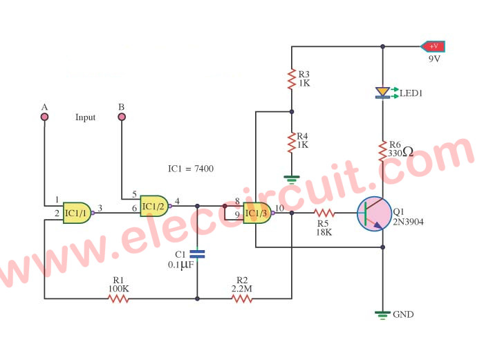
But if the A is listed as “1” and B is listed as “1” will enable LED1 blinking frequency of approximately 3.5 Hz.The principle is working. The first two legs of the conditions IC1 / 1 “0” to the output Into “1”.And IC1 / 2 off the output is “0” IC1 / 3 to return to the status output from a “1” LED1 is light.And caused a charge of C1.This will take and when will fully charge C1 pin 2 of IC1 / 1 is “1” makes the output from “0”.And IC1 / 2 off the output is “1” and IC1 / 3 to return to the status output from a “0” LED1 is extinguished. And caused the discharge of C1 through the voltage of R2 through the voltage of C1 gradually decreased.The voltage at pin 2 of IC1 / 1 to 0 volts of this work will continue, causing LED1 flashes.
Rising-edge trigger R-S Flip Flop circuit
The normal R-S flip flop circuit include of two nade gate are connected together and when need to set or reset then feed the logic signal is “1” instead trigger and use inverter work instead.
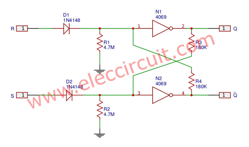
In Figure 1 suppose begin state of both input is “0” and output Q is “1”, input of N1 will be pulled to “1” by the 180 K resistors. Thus output Q so is “0”, that input of N2 is also “0”. Then if feed logic “1” to input s output -Q will be “0” pull input of N1 is also “0” and output Q will be “1”.
Thus input of N2 will be pulled as “1” Although input S is “0” another matter. And When feed logic “1” into the input R will reset the flip flop and Process change would be opposite to the above.
The R-S flip flop circuit should drive easily the load that has resistance of 180K at logic “1”. The CMOS circuit can drive the load on this already.
Digital logarithmic sweep signal generator circuit
This is a Digital logarithmic sweep signal generator circuit by using the average digital. It uses together with the frequency generator by voltage controller.
How Digital logarithmic generator works
In the circuit, the 14-bit binary counter circuit, that input is synced with the output of oscillator generator circuit. Then, the 8 output of IC-4020 is connected to the resistor networks, that will change the digital code to the DC voltage level.
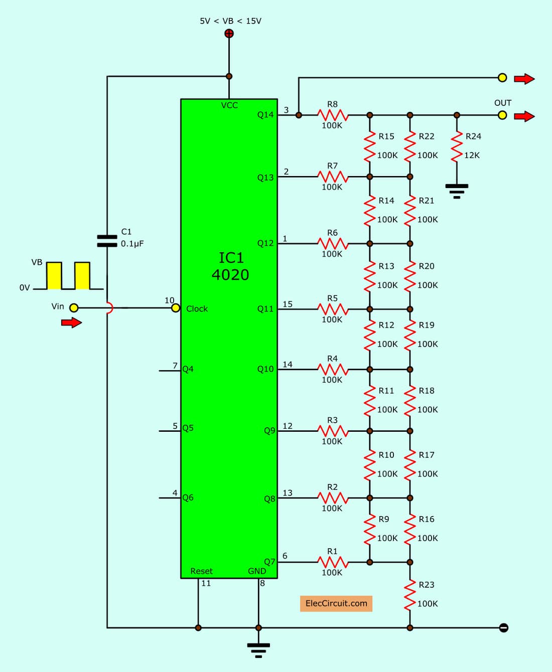
Thus, the DC voltage level from zero to about 0.2Vb. So it is divided into 256 steps. But lower output will not connects to any things. It cause the DC voltage level Uo increased step by step. After that, the clock through 128 cycle. This output can continue to sweep input of the oscillator is controlled by voltage.
A frequency generator from the circuit (And frequency synchronization output) increases every time the control voltage increases. This makes the voltage and frequency increased almost as exponential required.
When applying Uo from the oscillator controlled by voltage into Vin of this circuit. The resistor R9 the t input of IC2 must change to direct connect. Thus no logarithmic voltage at Uo, But it is only the output of IC2.
The circuit connecting
The circuit will connect two sections in together with adjusting as follows. To connects the reset wire to connect temporarily reset to IC4020, across reset pin to a positive voltage. Then, adjust the frequency at pin 11 of XR2206 take output is 80Hz.
Next, Disconnect the reset wires from the positive to ground instead. Then, adjust start bottom to “connected” the sweep frequency (the clock frequency of IC1) will start at lowest frequency (80 Hz) and long times about 1 Second. After that, the IC1 will increase the frequency in step by step until you reach 20 KHz.
The speed of sweeping can increase is 2 times, by connected to resistors R1 to R8. In the sweeping circuit, Q6 to Q13 replace output Q7 to Q14 and If move to Q5 – Q12 instead will can get speed up to 2 times. The speed of the basic clock can multiply with 8 by connecting output Q4 to Q11.
Bicycle distance meter circuit using 4N26,CD4017
This is Bicycle distance meter circuit or Measure the distance by use bicycle wheel as main tool and normal electronic circuits and so important parts are reed switch detect a magnetic force to CD4017 as Decade counter with 10 decoded outputs IC then connected to Optocoupler 4N26, and display to a frequency counter.

Two-wheel vehicle known as the bicycle is a vehicle that has been used for a long time. Not just items truck. Two foot spin took people to their destination only. But also as an exercise to the body. Strong mental health to boot. And currently has a campaign to turn the bike well. In addition to saving energy, then. Considered to reduce pollution to the environment.
The rotation of each wheel. Possible to calculate the length distance as Figure 1 Distance measuring circuit the principle detect rotation in each round. and Determine to rotate Fully 8 rounds. So will display the once.
In this case the diameter of the wheel is about 24-26 inchs. When rotated Fully to on 8 cycle distance of 0.01 miles, or about 16 metre. Calculate the circumference of a wheel. When rotated, the 8 round distance of 16 metre.
The working of circuit
The reed switch-S1 detect a magnetic force by it is connected circuit when has When the magnetic force approach. And turn on the circuit when When the magnetic field away working with resistors-R1, R2 and capacitors-C1,to generate pulse signal to IC1 Count the number of pulses. When count up to pulse No. 8 will have voltage “high” out of pin 6 through R4 to trigger base of transistor-Q1 to working, there are current flow through LED inside the optocoupler-IC2, then send the pulse signal output of pin 7, 8 to go a frequency counter module of distance meter that successfully installed on the bike.
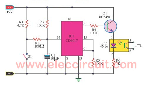
Figure 1 Measure the distance circuits
The magnet plate is stalled on a bicycle wheel. From the center of bicycle wheel about 12.5 inch. The reed switch-S1 is stalled at fork of bicycle in level matches the magnets plate. When magnet rotates matched switch-S1 is fully one cycle. Then, generate pulse signals up to one pulse.
If wheel full in 8 cycle. and will have pulse in to IC1 = 8 pluse. and there are voltage output to trigger to transistor works, then Display to the distance meter once time.
But when wheel rotates to 9 cycle or pulse no. 9 to IC1 will into reset mode or Restart again until full 8 turns. so It will show at the distance meter is second time. Each time the display out to a distance of 0.01 miles. or about 16 metre.
How to builds
This project has a few components so can assemble on the universal PCB board.
Starting equipment lowest first to the assembly. Start from Diode and then resistors and sort of high continuously.
The device has various polarity must be careful with setting the polarity at PCB and the part match together.
The soldering iron is less than 40watts. And Use of lead solder containing lead and tin in the ratio of 60/40. Including the need also to have a flux inside the lead.
Reed switch
The components list
Resistors size ¼W +5%
R1: 4.7K
R2: 100 ohms
R3-R5: 100K
R6: 1K
Capacitors
C1: 10uF 16V Electrolytic
Semiconductors
Q1: BC549C 45V 100mA NPN Transistor
IC1: CD4017, Decade counter with 10 decoded outputs IC
IC2: Optocoupler number 4N26
Others
S1: Reed switch
Small magnet plate
Universal PCB board
GET UPDATE VIA EMAIL
I always try to make Electronics Learning Easy.
Related Posts


I love electronics. I have been learning about them through creating simple electronic circuits or small projects. And now I am also having my children do the same. Nevertheless, I hope you found the experiences we shared on this site useful and fulfilling.
Thank you sir.
Hi Sayar
Thanks for your feedback.
What can be done to avoid between 1/3 and 2/3 Vdd when using analog signal as input? Thank you
Hello Adeyemi,
Thanks for your question. I am happy that you are interested in CMOS Digital ICs.
Even, it is so easy but so useful, too.
This problem can be avoided by using digital ICs with Schmitt Trigger features such as CD4093 Nand gate, CD40106 Inverter/Not gate. The output of these ICs has only 2 levels, “1” and “0”. Only. Even if the analog signal on the input is changed in any way.
If I have free time, will write more articles about them. Please wait for me.
Thank you, What can be done to avoid between 1/3 and 2/3 Vdd input voltage so that the ic will not malfunction when using it in circuit with variable input voltage?
Kindly post a CD4069 ic voltage stabilizer 5 relay circuit
“Kindly post a CD4069 ic voltage stabilizer 5 relay circuit”
Do you want The 5 relay control using CD4069?
Currently, I don’t have such a circuit. But it’s an interesting concept. I like simple experiments. to use and have knowledge At least teach the children. I will try your circuits. (when I get free)