This is a car 12V audio amplifier circuit that has high power over than 50w Using the IC TDA1562Q Philips. Which It uses just 12 volts power supply only. But provide higher watt power to 54 Wrms at load speaker 4 ohms and there is distortion at 1% and watt power maximum 65 Vrms at distortion 10%. The watt power this size suitable for install in our cars, since enough for speakers per channel and cheap
The quality was better than expected. Suitable for installation on all vehicles, Or if to build a power amps to listen to at home, was no problems whatsoever can be applications fully.
How it works
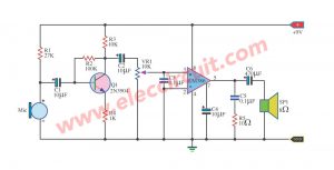
In Figure 1 is shown the 50W BCL 12v car audio amplifiers circuit, at pin 9 and pin 10 of IC1 into the power supply from the battery 12 volts. Then pin 6, 12 and 17 are connected to a negative voltage, there are two capacitors C7, C8 serves as eliminating interference and power backup for IC1, respectively. To make It run without distortion of the noise signal.
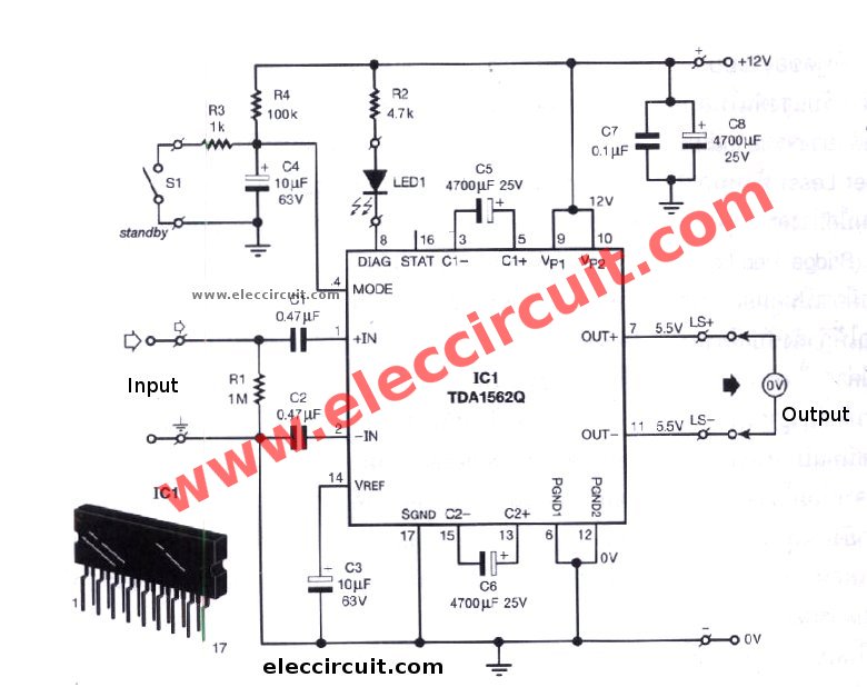
Figure 1 the 12V 50w audio amplifier using TDA1562
The sound signal input from the CD player, Tuner or output of the tone control as selecting. The input signal enters to C1, C2. Which are non-polar serves as coupling the sound signal? By can response the sound frequencies in 20 Hz to 20 KHz as well. And audio signals are sent to the pin 1 and pin 2 into IC1 so that amply the output to pin 7 and pin 11. Which pin 7 writes that the LS + refers provide the positive of the speaker. The pin 11 wrote that the LS-means connect to the negative of the speaker.
Is to be noted that terminal of the speaker will be connected to the ground of system. Since we know already that the circuit is connected to the bridge amplifiers. So If there are connecting a speaker cable wrong point or connected to ground. The detection system will immediately error. Resulting voltage pin 8 is close to the negative voltage, cause current flow through from voltage +12 volts, through to R2 cause LED1 glow to alarm user know the error.
If the operation of the circuit is normal, the voltage at pin 8 is very close to the power supply, cause the reverse bias so makes LED1 go out. (A resistor R2 that series with LED1 can be damaged if too little.But if an R2 value too much. The current through LED1 less does not see the brightness of LED1.
The lift level voltage circuit has connected the output to pin 3, 5 and pin 13, 15. To will be connected to the electrolytic capacitors C5, C6, to serves as boost current and voltage rises. makes power watts higher as well.
At pin 4 of IC1 consists of switch S1, R3, R4, and C4 serves as a select mode that will be Stand-by or Mute. Suppose that turn on switch S1 state now will prepare so that wait for a simple voice, Is turn on ready to work. But must delay before. Which takes about 1 second, wait for the capacitor C4 charges through R4 before.
The time delay is the symbol “T”.
Can calculate as follows.
T = R4xC4
When R4 and C4 are equal to 100 Kohms 10 microfarads.
Therefore, the delay time.
T = 100K x 10uF = 1 Second
The time delay is equal to 1 second.
But if turn off switch S1 now C4-capacitor will discharge through R3 to ground This condition will stop the sound. While in a state of IC1 stop this noise. The very low flow is 200 micro Amperes.
How to build it
Building this project. Has the same manner as other projects past. Until some of you Has tired so I say in conclusion, And this project uses less equipment and simpler.
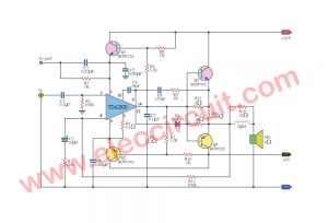
Starting from build PCB by Figure 2, and positioning all devices as the layout on Figure 3, Should abide by following steps.
1. Put three jumper wire below the IC. Followed by R1, R2, R3, and R4 soldered to it, because if not, the project may have a significant problem.
2. solder LED1, observe polarity so well, do not reverse certainly
3. solder the C1, C2, C3, C4, and C7.
4.Solder terminals And the eyelets at various points such as input, output and power supply After soldering the connector switch S1
5. Solder the electrolytic capacitors C5, C6 and C8 Notice polarity so well, do not reverse certainly
6. Against the power amplifier IC with Heatsink. Marked on the heat sink. To penetrate the IC. by the plan or mica insulation sandwiched. Solder pins of the IC carefully. Otherwise, the project may not work.
7. Check the short circuit or lack circuit, pins of the device, and modify immediately soon.
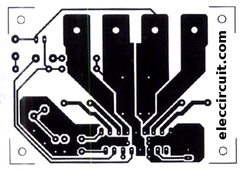
Figure 2 The single-sided PCB layout of 12v 50w audio amplifier
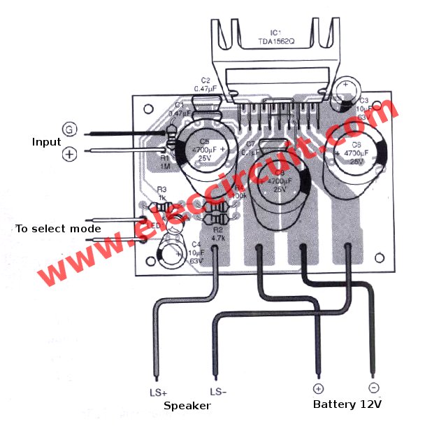
Figure 3 The Component layout for the PCB
How to test circuits
When the project finish, should test it, the steps are as follows.
1. Apply the power supply from battery 12 volts or voltage from the power supply that adjust DC voltage at 12 volts and provide current over 1 amperes, into the positive terminal of C8, and negative voltage at also negative of C8. Now must no burning smell and touch at IC1 must be cool. If error must disconnect the power supply immediately rushed out and quickly modify the project.
2. Measure a voltage at pin 7 of IC1 means LS + point by DC voltage range.
TDA1562 datasheet – 70w high car audio amplifier
The TDA1562 datasheet is a high output power 70W /4 ohms Bridge-Tied-Load(BTL) class H and AB high efficiency power amplifiers in plastic power package (TO-220)
The device can be used for car audio systems (e.g. car radios and boosters) as well as mains fed applications (e.g. midi/mini audio combinations and TV sound).
Technical specifications.
- power watts much high output the amply is determined in class H or class AB.
- Power loss or energy consumption is low.
- Short speakers are not broken.
- The Currents and temperature protection.
- On-Off operation without Currents surge.
- A display unit error.
- A few external parts.
- All switching levels with hysteresis.
- Protection short circuits across to ground.
- Thermal protection with parole circuit.
- Fast mute on supply voltage drops.
- Mode select are on, mute and standby.
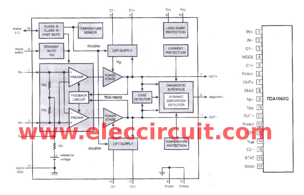
Figure the block diagram and pins to use of TDA1562
The results of measurements in practice.
- Can be used with a wide power supply of 8-18V absolutely no danger.
- The signal input is more sensitive 0.76V RMS.
- Impedance input is 75K Ohms
- Maximum power watts output is 54W RMS impedance speaker 4 ohms. Which tested with frequency 1KHz, with the distortion and noise, only 1% (f = 1kHz; THD + N = 1%).
- The frequency response is very wide of 7.5Hz – 185kHz Test driving a 25W load speaker 4 ohms.
- Currents in calm conditions is about 135mA.
- Ratio to the noise signal is equal to 88dBA.
- Low harmonic Distortion Noise (THD+N):
Testing value
- 0.046% at frequency 1kHz on load 1W @ speaker 4 ohms
- 0.29% at frequency 20kHz on load 1W @ speaker 4 ohms
- 0.12% at frequency 1kHz on load 35W @ speaker 4 ohms
- 0.7% at frequency 20kHz on load 35W @ speaker 4ohms
- (Pin ground of output and power supply were entirely separated.)
How to use Pins
- Pin 1 is a positive signal input.
- Pin 2 is a negative signal input.
- Pin 3 is connected to a raise the voltage level circuit, for the within amplifier 1, that negative of electrolytic capacitors.
- Pin 4 is mode select input that standby or sounds stop.
- Pin 5 is connected to a raise the voltage level circuit, for the within amplifier 1, that connected the positive of electrolytic capacitors.
- Pin 6 is a ground system that serves to get negative voltage.
- Pin 7 is the output pin with the positive terminal speaker.
- Pin 8 is a pin display to check errors.
- Pin 9, 10 are derived the positive voltage from a battery 12 volts.
- Pin 11 is output for the negative terminal speaker.
- Pin 12 is the ground pin of the negative battery terminal.
- Pin 13(C2+) is connected to a raise the voltage level circuit, for the within amplifier 2, that connected the positive terminal of electrolytic capacitor 2.
- Pin 14(Vref) is used for internal reference voltage.
- Pin 15 (C2-) is connected to a raise the voltage level circuit, for the within amplifier 2, that connected the negative terminal of electrolytic capacitor 2.
- Pin 16(STAT) is a status input/output of system.
- Pin 17(SGND) is the signal ground.
In block diagram within IC consists of the power amplifier on OTL : Output Transformer Less are 2 set as follow the preamplifier and main amps each 2 set. They are connected on the bridge circuit called Bridge Tied Load. As a result, the value of DC voltage at output speaker as zero why have the BTL circuit to Output Power a lot more loudly.
We want to maintain the stability of the system and completely eliminate noise signal. so has the Negative Feedback Circuit,by will connects from the output of the amplifier section to input of the preamplifier circuit. To troubleshoot various oscillator signal the preamplifier and main amplifier Can respond to frequencies from 7.5 HZ to 185 KHz. (Sound frequencies is the frequency range between 20 Hz to 20 KHz, but this good power amplifier has a wide frequency response.) Input signals into the pin 1 to pin 2, By pin 2 is the ground of the signal. Which is not related to the ground of the power supply itself.
The circuit that causes power watts output Higher up is a Lift Supply Circuit will connecting to the power amplifier As a result, the current and the voltage is increased. They has the circuit 2 set, By set 1 will connected to pin 3 and pin 5. Then set number 2 is connected to pin 13 and pin 15 of IC. Which is connected to the high large electrolytic capacitors to boost up the current and voltage value to this system.
Around pin 9 and pin 10 of IC serves as is drived the positive 12 voltage from the battery. The negative battery is entered at pin 6, 12 and pin 17. Since this amplifier is Mono channel. So the output of circuit will is send to pin and pin 11, and notice that speaker will not connected to any ground.
Related 12v audio amplifier Circuits
I love electronic circuit. I will collect a lot circuit electronic for teach my son and are useful for everyone.

nice circuit thanks……YC0LOG
50w public address system circuit based on IC with microphone input is required. please guide
Hello, What is the purpose the MODE pin ??
Purpose or function of mode pin ?
Where and how can l make an order for electronic components
i wanted to add a kill switch (to connect it to my head unit ) or a simple switch just to turn of the amp when not required or when the car turns of …how can i do this please suggest me with a wiring diagram its uregent
I have TB2904HQ ic can you publish working diagram of it thanks
please where can one get the ic.
Please try here: https://www.utsource.net/pro/TDA1562.html