We previously learned about the basic working principle of a buck converter. It’s interesting, but it’s a bit difficult to understand. We therefore recommend you make one of these an example of a step-down converter or a buck converter circuit.
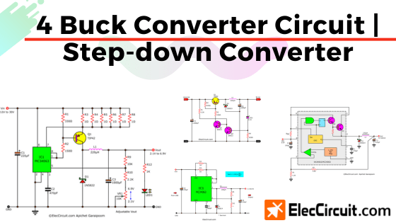
Transistor Buck Converter Circuit
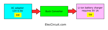
We have an automatic Li-ion battery charger circuit that requires a 5V, 1A input. But we only have the old 12V, 0.5A power supply circuit (AC adapter).
So we will use the buck converter to reduce the voltage to 5V and increase the current to 1A.
Note:
Currently, my daughter is studying transistors, so we wanted to try out the basic transistor circuit to solve this problem. It may not be a complete switching regulator circuit.
But at least we can learn the basics of the buck converter along the way. We also like to use our old components, and they can also be good teachers for us.
How it works
It looks similar to the series voltage regulator of a linear power supply. However, the series voltage regulator works like a resistor that always reduces the current to the load, whereas a buck converter can increase the current.
So due to the similarity in both circuits, we are going to use the series voltage regulator as a base and build off from there.
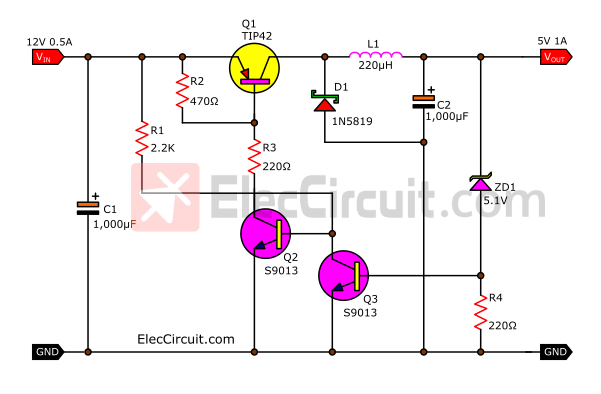
The main change we made was adding the inductor L1. It works as an excellent electrical energy storage tank, similar to a capacitor.
Another component of note is Q1, which acts as a switching unit that works with L1, D1, and Q2 transistors. Both NPN (Q2) and PNP (Q1) transistors will feedback each other to continuously switch and generate a frequency.
When we apply electricity to the circuit, Q2 will work. Because a base current flows through R1 to bias Q2 into the conducting state. As a result, the positive current flows through pin E to pin B of Q1 and flows through C-E of Q2 to the GND.
In this case, it means that Q2 is used as Q1’s bias controller so that Q1 can supply a high current through pin C to coil L1.
The pin B of Q2 is also connected to pin C of Q3, which has ZD1 and R4 connected to pin B to control the voltage to be approximately 5.2 volts.
The way it can achieve this is when the output voltage level exceeds 5.2V, the current will flow through ZD1 to pin B of Q3, causing it to conduct current between its C and E pins. Functioning like a closed switch, giving the current a shorter path through pins B and E of Q2. As a result, Q2 stops conducting current, and so does Q1, and the output voltage drops.
Now coil L1 will start releasing the current, and D1, which acts as a rectifier, will rectify the negative potential and then charge up C2 through its negative polarity. Until L1 runs out of current, the cycle will start over again.
Components List
This circuit has a few components, and they are all easy to find.
Here are a few electronic component lists that you can find anywhere.
0.25W or 0.5W Resistors, tolerance: 5%
- R1: 2.2K
- R2: 470Ω
- R3, R4: 220Ω
Electrolytic Capacitors
- C1: 1,000µF 25V
- C2: 1,000µF 16V
Semiconductors:
- Q1: TIP42 or equivalent, 100V 6A transistor
- Q2, Q3: S9013 or equivalent, 40V 0.5A Transistor
- D1: 1N5819, 40V 1A, Schottky Barrier Diode
- ZD1: 5.1V 500mA or 1W, Zener Diode
- L1: 220µH inductor coil
Recommended: If you are a beginner, read Electronic components list with images.
But there are some components that require extra consideration, including:
Inductor
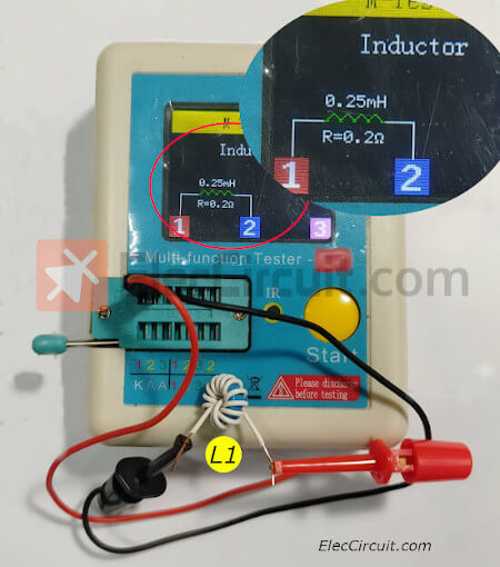
We made our own inductor L1 from a donut ferrite toroid core measuring 9.8 mm in diameter, 4.6 mm in ring width, and 5.9 mm in height. Then, wrap approximately 14 turns of 26AWG solid wire on the ferrite core. And we measured the inductance to be approximately 0.25mH or 250uH.
Diode
We picked the 1N5819 Schottky Barrier Diode as D1 because it has higher efficiency than using a regular 1N4007 silicon diode.
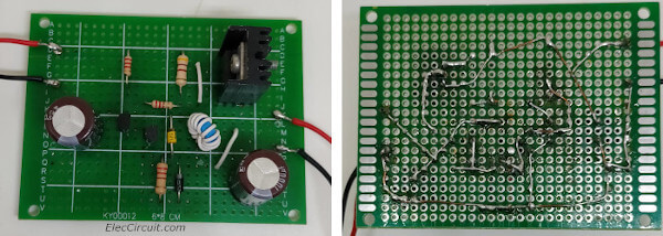
Then, we assemble the prototype circuit on a perforated PCB. Which is quite simple because there are not many components.
Testing this circuit
Once assembled, we test it out, as shown in the picture below. It worked quite well. The output voltage, when used with a Li-ion battery charger, drops to approximately 4.9V and can output approximately 1A. After nearly three hours, the battery was fully charged.
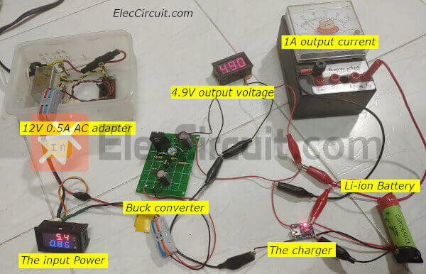
Testing the circuit with the Li-ion battery charger.
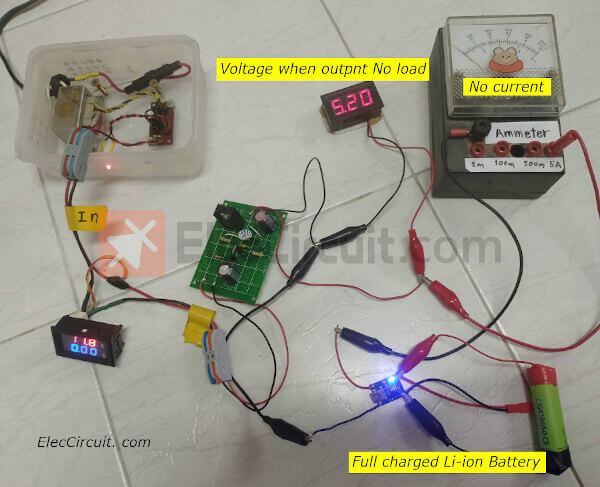
The voltage level of the Buck converter returned to 5.2V when there was no load.
Disadvantages of this circuit
Note: When there is a load, the input of the Buck converter is approximately 5.4V at 0.9A, and the output voltage is approximately 4.9V at 0.8A. It loses about 20% of the energy inside the Buck converter. It is not a complete switching regulator with about 90% or more efficiency.
This 5V buck converter circuit, although it is similar to a linear regulator, worked adequately. It can provide a constant voltage level of 5.2V when there is no load and up to 4.9V with a load that uses a current of approximately 1A. And it can be used continuously for a long time, with Q1 not getting hot either.
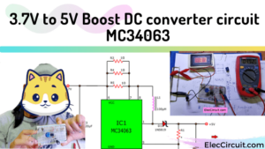
However, if you are looking for a circuit for day-to-day use, you should choose an IC, such as the MC34063, because we can determine the output voltage easily and accurately, and it has high efficiency with various protection systems.
Simple 5V Buck Converter Circuit
This is simple 5V Buck Converter Circuit or the 5V 500mA Switching Regulator Circuit. It can be placed in the buck converter category, hence the name. This circuit has a higher efficiency than a linear regulator.
For instance, if supplied with a Vin of 21V 100mA, it will have enough capacity to drive a 500mA load.
We will briefly learn it first, just enough for us to use it. In the future, my daughter and I will learn more deeply about it, and we will tell you more about that experience.
If you are a beginner, you should learn the working principle of a basic buck converter first.
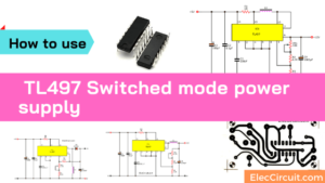
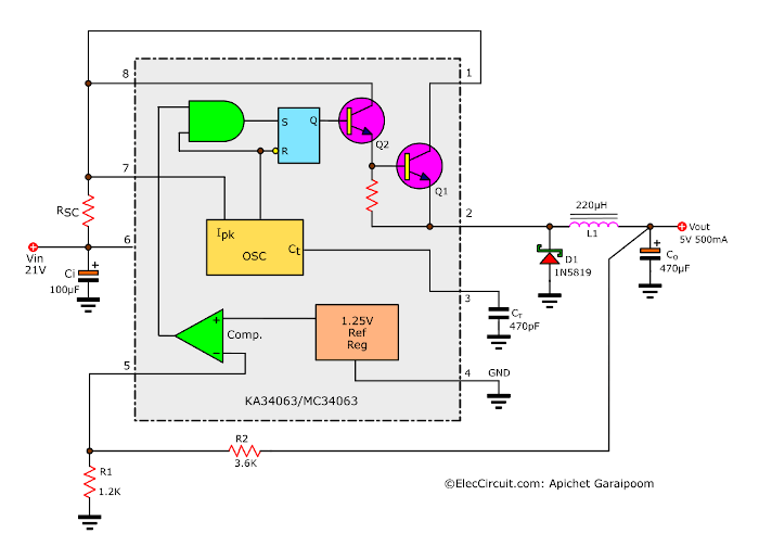
But to put it simply, it consists of Ci, Co, L1, D1, and the switching system, which is inside the chip.
Look Inside working
Its switching system comprises several parts.
Q1 and Q2 are transistors run as switches at high frequencies, controlled through RS flip-flops generated by an oscillator.
The OSC’s frequency is determined by CT at pin 3. In the datasheet, it is suggested that CT be 470pF, while pin 3 measures approximately 30kHz at no load.
The output voltage is determined by R1 and R2, whose values can be calculated by the following formula: Vout = 1.25 V x {1 + R2/R1}.
RSC is a max-current limit resistor. In this case, the RSC is 0.3 ohms, as it will limit the current at 1A through the formula 0.3V/0.3 = 1A. But at normal operating efficiency, it can only power about 0.5 A of current.
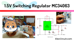
1.5V/3V Buck converter circuit
Next, it is a 1.5V/3V Buck converter circuit. The output voltage can be set with R1 and R2 see in table below.
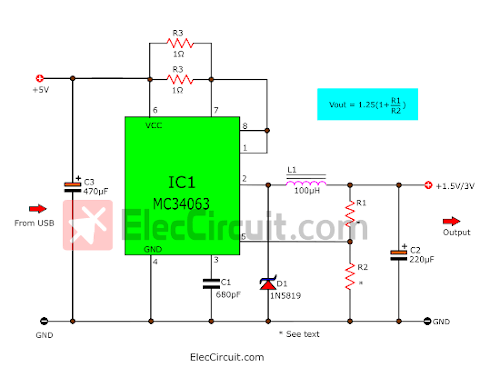
| Voltage Output | R1 | R2 |
| 1.5 V | 100Ω | 470Ω |
| 3 V | 470Ω | 330Ω |
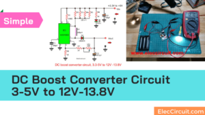
5V 2A Buck converter circuit
Suppose that we are in an area with no electricity. With this 5V 2A buck converter circuit, we can charge our mobile phone with a 10W solar cell that can supply a current of approximately 0.5A and a voltage of 17V to 21V.
It can supply a voltage of 5V and a current of 0.6A to 1.8A to charge our phone with just the solar cell that we have.
This block diagram below will help you visualize the order of operation more easily.
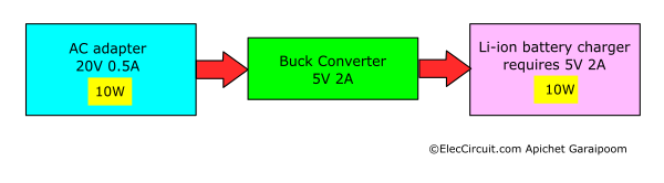
The buck converter can convert almost the same amount of power. In practice, its output may be reduced to 9W, which results in us having to wait longer to charge the battery.
However, this loss rate is acceptable because it is very low.
Increasing current with PNP Transistor
By adding a transistor, we can amplify the current higher. According to its datasheet, we can use both NPN and PNP transistors, but we should use PNP transistors instead because it has higher efficiency.
We’ve also added R1 and R2 to help optimise the bias current. As for the transistor, we chose the TIP42 because its datasheet says that it can drive current up to 6A.
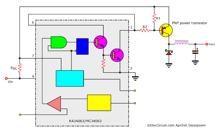
Through our experiments, we can infer that we can increase the current to approximately 2A, with R1’s and R2’s values being 330Ω and 150Ω, respectively.
We can also use MOSFETs to increase the current.
5V 2A Buck converter circuit works
And finally, let us take a look at our complete circuit below.
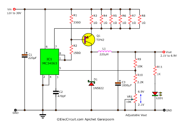
Which has additional details as follows:
L1 (inductor): we use a size of 220uH that can withstand a current of 3A. You should not be using anything lower than this because it causes the current to decrease.
C3 (CO-output capacitor): we use 1,000µF at 16V to reduce the output ripple voltage to approximately 30mV or less. Do not use one with a capacity lower than this, as it will reduce the output voltage when using a high-current load.
C1 (Ci-input capacitor): we use 220µF at 35V; it’s improves the efficiency of the circuit. When the input voltage fluctuates rapidly. It should keep the DC working voltage (WVDC) at least 35V because we use an input voltage of 30V maximum.
C2 (Ct): we use the original value of 470pF.
D1: We use 1N5822 because it can withstand a high current of 3A, enough for our use here of 2A.
RSC (Max Current Limit Resistor)
When we set the maximum current at 2A. The RSC’s resistance is calculated to be 0.15Ω. But we currently do not have a resistor of that value.
So we connect six 1Ω resistors in parallel until we get the total resistance of 0.17Ω.
When rechecking our work, it shows that with our current setup, the max current is 1.76A; according to this formula, 0.3V/0.17Ω = 1.76A. Which is enough to charge the battery.
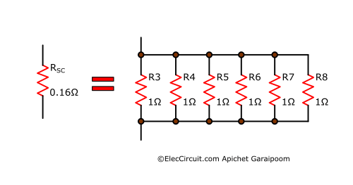
In the circuit, the RSC is R3 to R8.
Set the Output Voltage
We want the output voltage to be exactly 5V. From the formula given by the manufacturer, Vout = 1.25 V x {1 + R2/R1}.
But this only resulted in a constant output, so if we want it to be adjustable, we simply need to add variables in the form of a potentiometer in series, as shown in the illustration below.
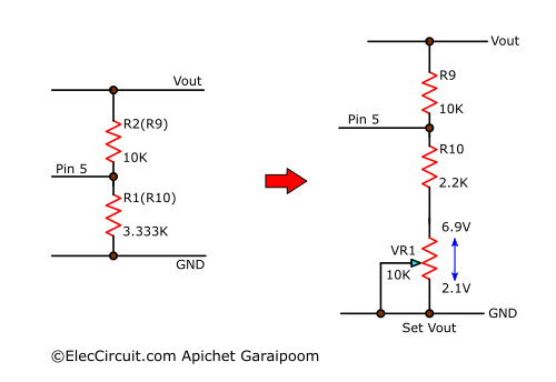
Allowing the Vout to be adjusted to any voltage in the range of 2.1V to 6.9V.
So now this circuit can be anything from a 3V Buck Converter Circuit to a 6V or even a 4.5V 2A Switching Regulator Circuit just by tweaking VR1.
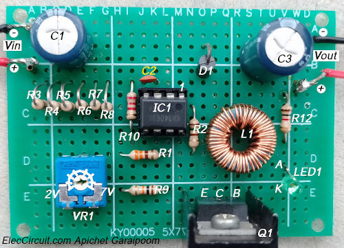
Building 5V 2A Buck converter circuit
This circuit only has a few components, and they are all easy to find.
Components List
Resistors; 0.25W or 0.5W, 5% tolerance
- R1: 330Ω
- R2: 150Ω
- R3 to R8: 1Ω (8 pcs.)
- R9: 10K
- R10: 2.2K
- R11: 1K
- VR1: 100K Trimmer Potentiometer
Capacitors:
- C1: 220µF 50V, Electrolytic
- C3: 1,000µF 16V, Electrolytic
- C2: 470pF 50V. Ceramic
Semiconductors and others:
- IC1: KA34063 or equivalent, Boost/Buck DC/DC Converter/ Switching Regulator
- Q1: TIP42 or equivalent, 100V 6A transistor
- D1: 1N5822, 40V 3A, Schottky Barrier Diode
- ZD1: 5.1V 500mA or 1W, Zener Diode
- LED1: 3mm Red LED
- L1: 220µH inductor coil at 3A current
- 5x7cm Perforated PCB
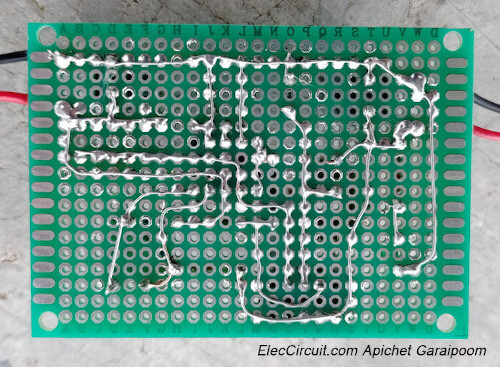
Now we assemble each component into the perforated PCB and wire them together in the same layout shown below.
Testing the circuit
We will be testing the circuit with a DC power supply supplying 21V 0.5A instead of the intended solar cell panel because it is easier to control and monitor.
Then we use a 470 ohms 2W resistor as a load with the setup shown below.
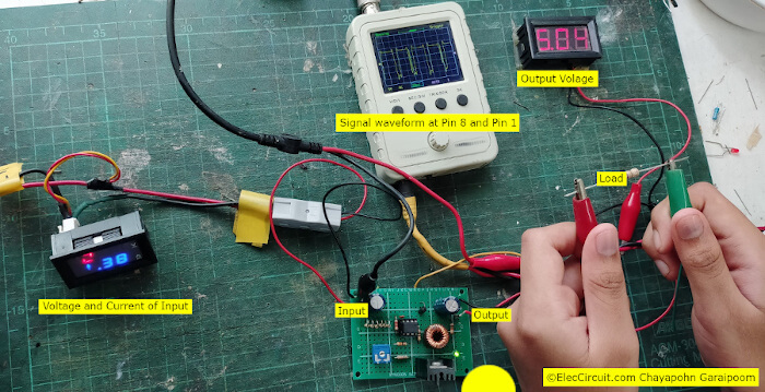
The output voltage remained at around 5.04V, while the input is 21V 0.38A.
Note that when we measure the frequency between pin 8 and pin 1, we see that it is in almost square-wave form with a frequency of about 30kHz. However, when the load’s size increases, the frequency will go up to 150kHz.
Now we try changing the load to one that requires 1.8A of current. And as shown below, the output voltage drops to 5.00V and the input current increases to 0.59A.
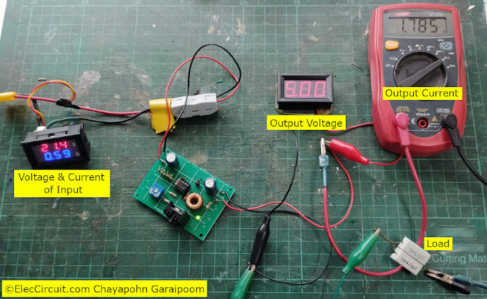
We may summarize both runs in a comparative table.
| Vin | Current in | Power in | Vout | Current-out | P-out | Efficiency % |
| 21V | 0.28A | 5.88W | 5.04V | 0.92A | 4.63W | 78.7% |
| 21V | 0.59A | 12.39W | 5V | 1.78A | 8.9W | 71.8% |
Theoretically speaking, it should have a higher efficiency of around 90% or even more. But this might be affected by components such as inductors, MOSFETs, etc.
Conclusion
We tested this circuit several times, and it worked quite well. The output voltage remains constant at 5V with a maximum current of about 2A. However, the input current must be greater than 0.6A at a voltage of about 20V. If our solar panel receives full sunlight for about 3 to 4 hours, it can fully charge our mobile phone.
In the future, we might use this Buck converter again. But especially for a larger load like a water pump, which needs 12V 40W, whereas our solar cell could supply a maximum of 21V 40W. Which should not be connected directly because the voltage is too high.
GET UPDATE VIA EMAIL
I always try to make Electronics Learning Easy.

I love electronics. I have been learning about them through creating simple electronic circuits or small projects. And now I am also having my children do the same. Nevertheless, I hope you found the experiences we shared on this site useful and fulfilling.