Today we are going to check out a triangle wave generator circuit that uses just a small electronic component. It can also generate a square as well as a triangle wave at the output. I made this a while back to learn about CMOS gates and an astable multivibrator.
And it has been very useful. So now I will recommend it to my daughter so she can learn from it, as I did.
I like it, as it is the first triangle wave generator circuit that I’ve made. It can give out two ranges of signals: a Low (or 10Hz-100Hz) and a High (or 1kHz-10kHz) range. And the voltage supply range is very wide, from 3V to 15V. The main components are a CD40106 Schmitt Trigger CMOS, an NPN transistor, and an RC.
I could adapt this circuit for work such as testing amplifiers, DC-to-AC inverters, and some others. We can also modify its waveform into a sine wave with ease. It is one electronic circuit that is very interesting to try.
Any kind of learning should be practiced gradually. Similar to planting a tree, we should water it gradually and continuously. because this tree (my daughter) has a short memory and a poor brain haha…
The Working of the Triangle Wave Generator
We should start with the basic Oscillator using the Schmitt trigger. The IC1-CD40106 is a CMOS Schmitt-Trigger Hex Inverter type IC. It will output a square waveform, where the frequency is determined by the values of R1 and C1.
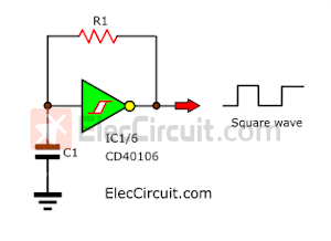
Or, to be exact, the frequency normally depends on the charge and discharge times of the capacitor. So if the capacitance and resistance increased, the output frequencies would reduce.
From my experience, R1 should be around 10K to 1M, and for C1, it should be around 100pF to 1μF.
We added other components until we got the circuit shown below.
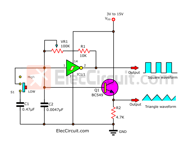
Meet the Triangle Wave Generator Circuit
The square waveform signal at output is determined by R1, VR1, C1, and C2, similar to the circuit above.
We add the switch S1 for choosing between frequency ranges between “high” and “low.” When S1 is on “low,”, capacitor C1 will connect with capacitor C2. Both capacitances will increase, causing the output frequency to be in the “Low” range and we can rotate VR1 to set the frequency from 10Hz to 100Hz.
But when S1 is “high”, this time there will be only one capacitor C2 that is connected at the input (pin 1) of IC1. This causes the output frequency to be in the “High” range, and we can rotate VR1 to set the frequency from 1KHz to 10KHz as well.
The triangle waveform has been derived from the charging and discharging of the capacitors (C1, C2) at pin 1 of IC1. To prevent loading those capacitors, there should be a simple buffer. which, in this case, will be a transistor Q1, as its common collector form.
The output is the same voltage as the drop across R2. The lowest point in the amplitude of the waveform will be higher than the zero voltage of the power supply.
Adjusting VR1 will change both the frequency of the square waveform and triangle waveform by the same amount.
The components list
- IC1: CD40106, CMOS Hex Schmitt-Trigger Inverters
- Q1: BC549, or equivalent, 45V 0.1A, TO-92 NPN Transistor
- R1: 10K, 0.25W Resistors, tolerance: 5%
- R2: 4.7K, 0.25W Resistors, tolerance: 5%
- VR1: 100K Linear Potentiometer
- C1: 0.47µF 50V, Ceramic Capacitor
- C2: 0.0047µF 50V, Ceramic Capacitor
- S1: SPDT Mini Micro Slide Switch
- Miscellaneous, Breadboad, Wires,
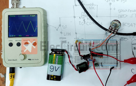
Building and testing
This circuit has a few devices. So we can assemble it on the small breadboard.
After reviewing the circuit, it is good. Then we feed it a 9V battery. This produces a square signal with an amplitude of about 6Vp-p.
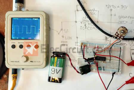
A triangular signal has an amplitude of approximately 1Vp-p at all frequency ranges it’s capable of.
Conclusion
This circuit has the disadvantage of a low current. but you can mitigate this by adding an amplifier. While still keeping the same signal format and frequency. At our next opportunity, we will try to build this amplifier circuit.
It is also a good idea to add short-circuit protection at the output.
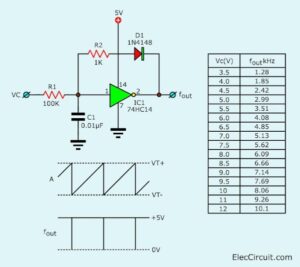
The triangular wave signals can also be turned into sine wave signals. In the future, it might be worth revisiting and modifying this circuit again.
Additionally, you may use other transistor families such as 2SC1815, 2N3904, S9013, and others. But their pins will not match; therefore, you should be especially careful when using them.
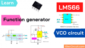
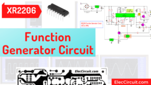
For example, the Function Generator
Download This
All full-size images and PDFs of this post are in this Ebook below. Please support me. 🙂

I love electronics. I have been learning about them through creating simple electronic circuits or small projects. And now I am also having my children do the same. Nevertheless, I hope you found the experiences we shared on this site useful and fulfilling.

hello all
can you just put the formula of the frequency?
i mean how it can be calculated
thank you
Nice circuit. Small & cheap!
Hello Prajit,
Thanks for your feedback. I am happy you like it.
JEG SKAL SE DET IGENNEM – JEG ER IKKE NYBEGYBDER .
VENLIG HILSEN WILLY
Hello Willy Petersen,
Thanks for your visit to my site.
Please tell me in English. I use Google translate. But cannot understand you.
Have a good day.
I wasn’t expecting to resonate so much with this article, but you captured the nuances of the topic so well. Thank you for your perspective.