When it came to the analog switches in a digital circuit, most people thought of the CD4066 or 74HC4066, as both utilized a silicon gate CMOS technology to drive their high-speed quad logic gates that are controlled by an external logic signal.
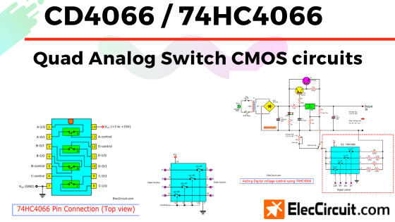
CD4066 / 74HC4066 Features
Inside of the 74HC4066, or 4066 in general, are four independent high-speed switches that can control either digital or analog signals with low power loss. It can also be used in both CMOS and TTL applications.
For example, if we give switch block A “high” logic by connecting the A control pin to the VCC, the A switch will turn on or close-circuit. This allows electrical currents to pass through both I-O and O-I.
On the other hand, if we connect the A control pin to GND, switch block A will receive “low” logic. This means that, unlike before, the A switch will turn off or open-circuit, preventing electrical current from flowing through the switch block A.
CD4066 / 74HC4066 Pinouts
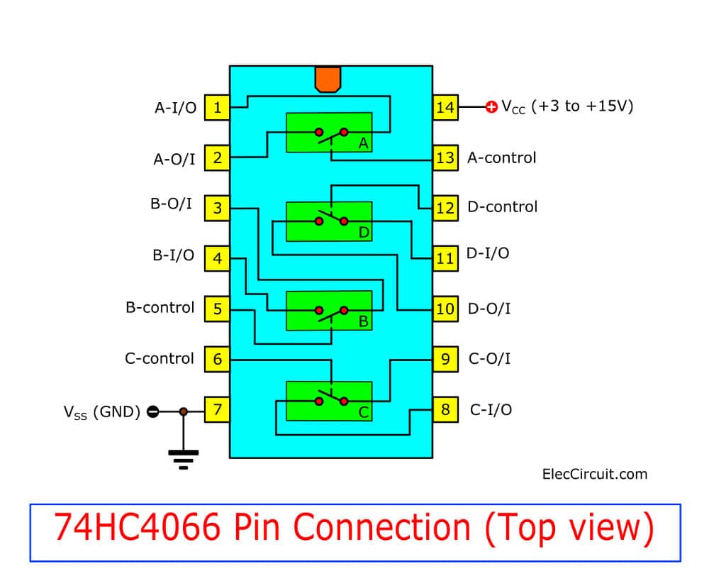
We can use 4066 easily. It looks like 4011 NAND gate CMOS. They are the same shape, DIP-14. But pinouts are different.
Specifications
- Wide supply voltage: 3V to 15V
- Use low supply current in CMOS technology
- Wide analog input voltage range: 0 to 12V
- High Speed: 7nS at Vcc = 5V
- Low Power Dissipation: 1uA(max) at Ta = 25°C
- High Noise Immunity: Vnih = Vnil = 28% Vcc(Min)
- Low ON Resistance: Ron = 50Ω at Vcc = 9V
- High OFF Resistance: 10M
- High Degree of Linearity THD = 0.05%(typ) at Vcc = 5V.
- Pin and Function Compatible with 4066B
- Frequency Response = 40MHz~
Buy CD4066 at Amazon.com HERE
Example CD4066 Circuits
Let’s see the example circuits. They may be good ideas for you.
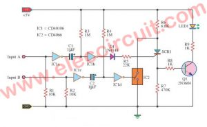
Signal bus controller circuit using CD4066
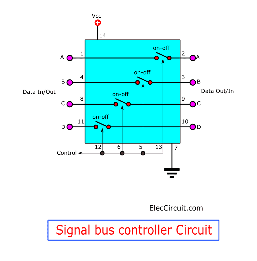
This is a data bus controller circuit. All of its control pins were merged together, meaning that all port data are controls all at once. So if we apply a “high” logic, signals can go in and out on all ports; on the other hand, when we apply a “low” logic, no signal can flow through.
Data selector circuit
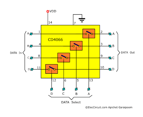
We can easily select an input data by simply entering a “high” stage to the DATA select pin. All three other DATA select pins are “Low” stage.
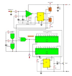
Adding digital voltage control
From the 3A adjustable power supply using LM317 and 2N3055.
Suppose that we want to change how we adjust the output voltage to a digital control or any logic signal, for example, the Arduino or others.
When logic “high” is applied to one of the four controls, the output voltage will change to either 3V, 6V, 9V, or 12V according to the predetermined voltage of that pin.
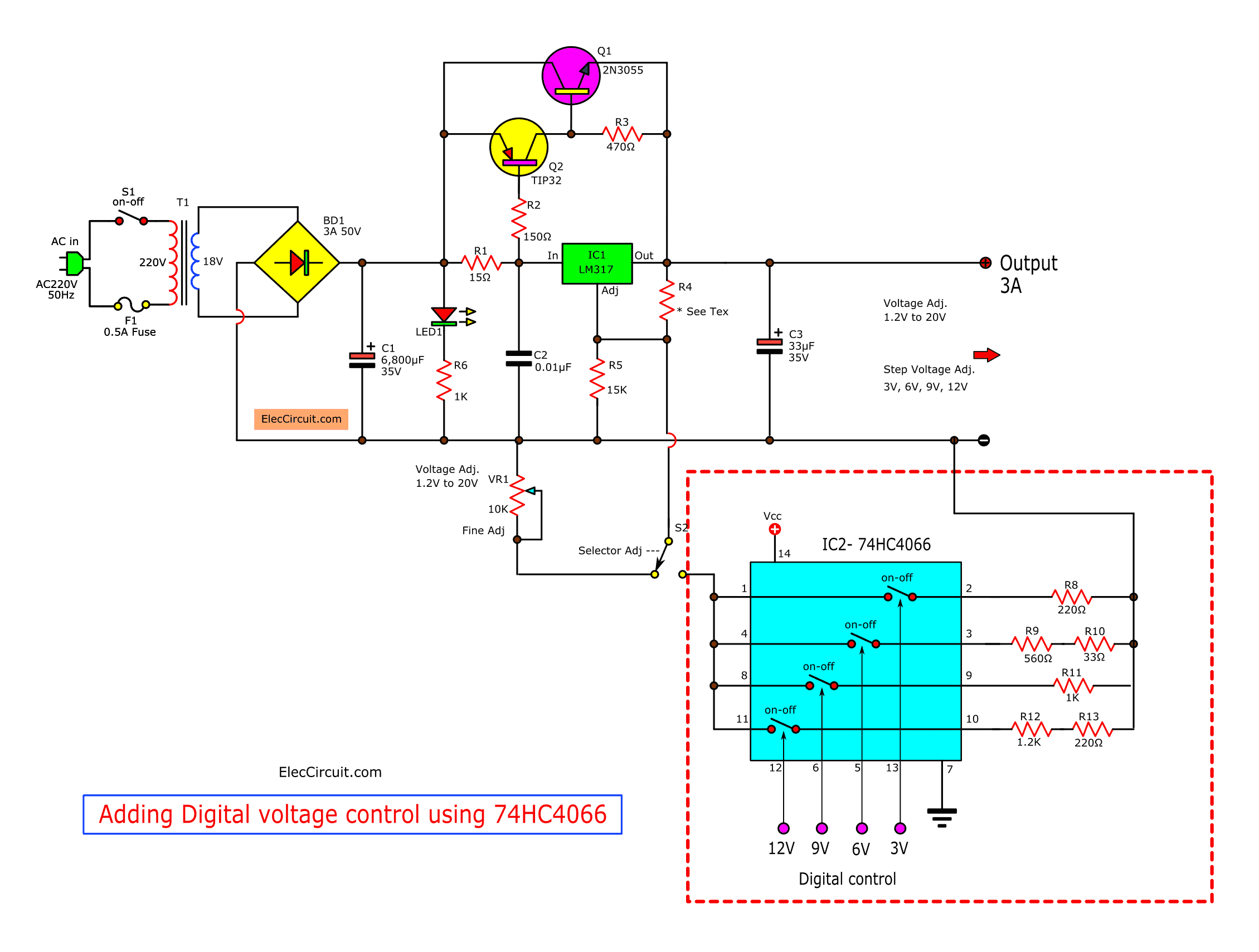
Also, this IC requires a 5V power supply to operate, so you might have to add one externally.
GET UPDATE VIA EMAIL
I always try to make Electronics Learning Easy.

I love electronics. I have been learning about them through creating simple electronic circuits or small projects. And now I am also having my children do the same. Nevertheless, I hope you found the experiences we shared on this site useful and fulfilling.