
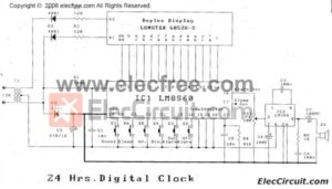
Today I highly recommend the alarm digital clock Another interesting project. Suitable for beginners It is small, easy to build, use IC number IC use LM8365 is at the heart. Includes all functions within a single IC. Thus, it is more efficient than this project, read below:
Feature:
- Designed as Model all parts on one PCB
- Show times is AM and PM
- Can set times alert 2 times in 24 hour
- Can schedule appliance to 1 hour.
- It has the backup battery when power outage this clock non stop.
- Can show dates, months or seconds
LM8365 functions of various pins and applications
-Pin 1_Alarm2 O/P is pin output of 2nd alarm
-Pin 2_AM O/P is pin output drive an AM display point
-Pin 3_10 Hrs b&c is pin connect to LED display ten digits of hours segment b&c
-Pin 4 HRS-f to pin 10 HRS-e are pins to LED display unit digits of hours sorting segment fe.
– Pin 11 10MINS-f to pin 16 10MINS-c are pins drive the LED display the ten digits of minutes to sort segment from fc.
– Pin 17_MINS-f to 23 MINS-c are pin to drive the LED display unit digits of minutes to sort segment from f-c
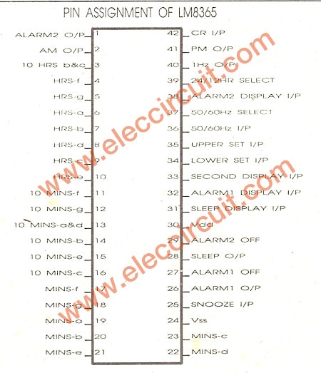
Figure 1 the functions of the various pins
– Pin 24_Vss is pin connect the positive power supply voltage
– Pin 25 SNOOZE I/P is input of the SNOOZE pushbutton switch which is connect to the positive voltage through switch to To stop the alarm, while about 9 minutes
– Pin 26_ALARM 1 O/P is pin output of the first alarm
– Pin 27_ALARM 1 OFF is pin connect to positive voltage to switch to stop the first alarm
– Pin 28 _SLEEP O/P is output of setting the appliances for long 1 hour
– Pin 29_Alarm 2 OFF is pin to connect the positive voltage switch to stop the 2nd alarm
– Pin 30_Vdd is Ground
– Pin 31_SLEEP DISPLAY I/P is pin positive to through switch to read times in setting the appliances
– Pin 32 ALARM 1 DISPLAY I/P is pin connect the positive voltage to switch to read times the first alarm
– Pin 33_SECOND DISPLAY I/P is pin connects the positive voltage through switch to press to look time in seconds
– Pin 34_LOWER SET I/P is pin connects the positive voltage through the switch to press to look time in minutes
– Pin 35_UPPER SET I/P is pin connects the positive voltage through the switch to press to look time in hour
– Pin 36_50/60 Hz I/P is pin connect the time base 50/60Hz frequencies
– Pin 37_50/60Hz select is pin to connects selects the times bases frequency. If want 50 Hz to the positive and when you want 60Hz to ground
– Pin 38_ALARM 2 DISPLAY I/P is pin connects the positive voltage through the switch to look the 2nd times setting
– Pin 39 24/12HR SELECT is pin to select display in 12 hour or 24 hour. If you leave floats or to the ground is a 12 hour. and If connect to positive will be 24 hour.
– Pin 40 1Hz O/P is pin output to connect to LED display show flashing in second
– Pin 41 PM O/P is pin output to drive LED display at pot PM
– Pin 42_CR I/P is pin connect to the positive voltage through the switch to press clear times setting
How it works
In circuit diagram as Figure 2 at pin 37, which is pin 50/60Hz, Selected to ground, show that this times base is 60Hz.
The Pin 39 floating, show that the circuit to display a 12 hour.
The pin 33 floating, indicating that the circuit is not displays a value of seconds. It can be used by itself to the positive voltage to switch through to look seconds.
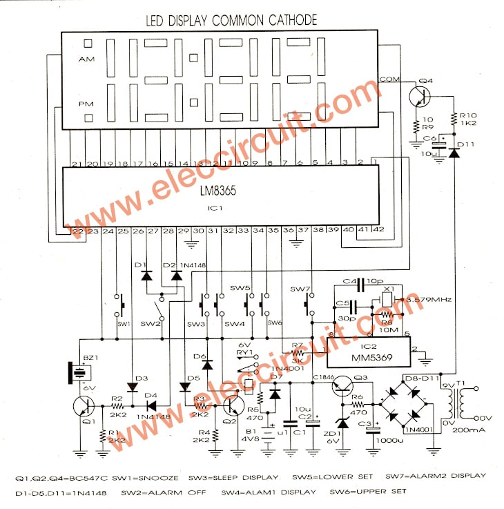
Figure 2 The schematic diagram of this project.
The pin 42 floating in a clear show that no set time.
Various switch functions are shown below the schematic diagram.
The note is at SW2, a switch Alarm OFF have D1 and D2 connect to through to switch to the positive voltage by connecting pin Alarm 1 and Alarm 2 O/P show that SW2 can use together to stop first alarm and 2nd alarm by all in one switch.
Recommendations for the switch SW2, should be ON / OFF, because if is normally open pushbutton the clock will alert every 24 hour.
D3 and D4 connects the output of alarm both 2 pin are pin 26 and pin 1. Connect driver Buzzers.
The pin 28 is pin SLEEP O/P connects to D5 the relay driver, by have Q2,R3 and R4 are the relay driver circuit.
There are D6 block is the voltage that will happen, If the power feed to the relay will stop the magnetic field collapses, cutting a relay coil voltage across the relay coil. This voltage can damage other equipment in the circuit.
The diode D6 will short circuit this voltage.
The terminal point the relay NO and NC must to connect to voltage 220VAC through contact NO and COM, to control timer the appliances for 1 hour
IC2 number MM5369 is an IC Clock Generator 60HZ. Which is the times base of IC1, the X-Tal 3.579 MHz is the frequency output 60Hz, connect to output pin 1 through R7 to pin 36 of IC1.
The Q3, R6 and the Zener diode ZD1 / 6V are connected the regulator circuit saving by three parts, Makes it voltage of the regulator circuit to maintain a constant cycle of approximately 5.4V.
It works as follows: R6 and ZD1 series causes a constant voltage of 6V the Zener diode. This point is connected to pin B of Q3 makes the voltage at pin B is steady.
Generally, when we have to maintain the voltage at pin B. The voltage at pin E will be steady, which led to the basic regulator circuit and saving.
But when transistor works, Q3 which is NPN type the voltage at pin B will be must higher than pin E about 0.6V. Thus the voltage at regulator so have 5.4V. Which is sufficient for the operation of the circuit R5 and D7 connected to backup battery circuit is 4.8V.
When power voltage 4.8V from battery will feed to D7 in to circuit instead voltage from the regulator circuit. But when the voltage remains normal, the voltage from the regulator circuit will be higher than voltage from battery, stop flow into the voltage circuit from the power supply will through R5 into charge battery instead.
Recommendations for the battery, should be the nickel cadmium battery in series 4 pcs. Q4,R10,C6 and D11 connected to get the voltage from terminal transformer is bias to transistor Q4 connect to common of LED display to ground through to R10. When power outlet, Q4 will stop working , make pin COM of LED display unconnected to ground of LED display to saving the power of backup battery.
How to builds
All components are installed on one PCB so easy to builds as Figure 4 and Figure 5 Then check the validity. It can be plugged into use immediately.
Caution: Need to put Q3-2SC1846 correctly
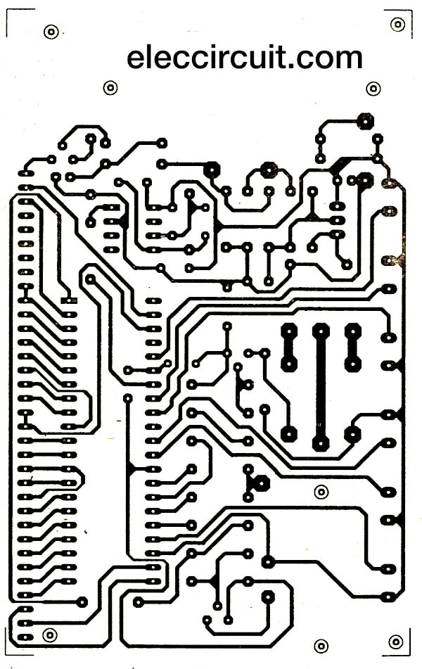
Figure 3 the PCB layout of LM8365
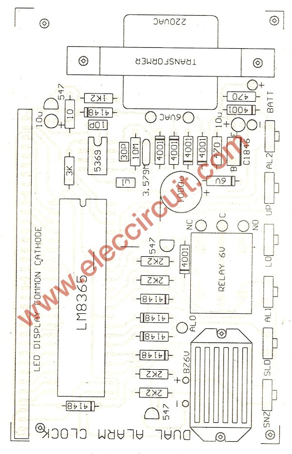
Figure 4 the components layout
Parts you will need
0.25W 5% Resistors
R1, R2, R3, and R4: 2.2K
R5,R6: 470 ohms
R7: 3K
R8: 10M
R9: 10 ohms
R10: 1.2K
Electrolytic Capacitors
C2, C6: 10uF 16V
C3: 1000uF 16V
Ceramic Capacitors
C1: 0.1uF 50V
C4: 10pF 50V
C5: 30pF 50V
Semiconductors
IC1: LM8365
IC2: MM5369
D1 – D5 and D12: 1N4148 Diode
D5 – D11: 1N4001 Diode
Q1, Q2 and Q4: BC547C
Q3: 2SC1846
ZD1: 6V 1A 0.5W Zener diode
Others
X1: X-Tal 3.579MHz
BZ1: 6V buzzer
RY1: 6V Relay
T1: 9V,200mA transformer
and more
GET UPDATE VIA EMAIL
I always try to make Electronics Learning Easy.
I love electronic circuit. I will collect a lot circuit electronic for teach my son and are useful for everyone.
श्री मान जी, नमस्कार,
मुझे आपके इस LM 8365 digital clock circuit का कुछ सामान चाहिए।
01- IC LM 8365,
02- PCB,
03- Display FND,
04- Buzzer वगैरा
तो ये सब मुझे कैसे मिलेगा ?
कृपया मुझे अपना Address व फोन नम्बर देने की कृपा करें।
Thanks
Surender Dhiman 8053551571
I want complete kit for LM8365 digital alarm clock. Can I get it by post? If yes please let me know it’s cost. I can pay on line or on delivery.
I like electric circuit
Hello Akeel,
Thanks for your feedback.
I want to get the total kit of LM8365 alarm digital clock from you. How to purchase? Please let me know.