Today we would like to introduce you to the CD40106 hex inverting Schmitt trigger. This chip is manufactured using the CMOS technology, akin to the CD4069 and CD4049 that we have talked about before.
Let’s see what made the CD40106 different from the others, its characteristics, its features, and its pinouts, together with a couple of example circuits down below.
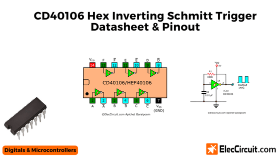
CD40106 Hex Inverting Schmitt Trigger
As the name suggests, the CD40106 contains six independent Schmitt trigger inverters or NOT gates. It can operate with an input range of 3V to 18V. This chip is often used to make an oscillator, function generator, and squarewave shaper or converter.
Being a Schmitt trigger means that the input voltage threshold for the output to switch from “high” to “low” is different from “low” to “high.” And of course, the inverting means that the output is inverted to that of the input.
Features
The CD40106 has many interesting and useful features; here are a few of them.
- Schmitt-trigger action requires no external components
- Hysteresis voltage of 0.9V, 2.3V, 3.5V at 5V, 10V, 15V input, respectively
- 5V, 10V, 15V rated input voltage
- Noise immunity greater than 50%
- No limit on input rise and fall times
- Symmetrical outputs
- Schmitt-trigger inputs
- Rated operating temperature from -40°C to 125°C
Pinouts
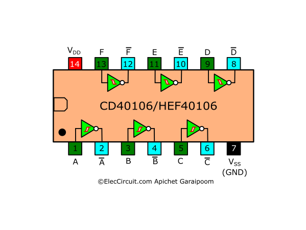
| Pins | Pin Types | Pin Functions |
|---|---|---|
| 1 | IN | A input |
| 2 | OUT | A inverting output |
| 3 | IN | B input |
| 4 | OUT | B inverting output |
| 5 | IN | C input |
| 6 | OUT | C inverting output |
| 7 | Power | Ground (VSS) |
| 8 | OUT | D inverting output |
| 9 | IN | D input |
| 10 | OUT | E inverting output |
| 11 | IN | E input |
| 12 | OUT | F inverting output |
| 13 | IN | F input |
| 14 | Power | Power supply (VDD) |
Specifications
In our experience, the CD40106 can withstand an input voltage (VDD) range of 3V to 18V. However, it is recommended that the VDD not exceed 15V and must be in the right polarity.
Each inverter gate can supply a current of about 10mA, which is enough for a 3mm LED. The CD40106 also has a supply current of 50 mA and an overall power dissipation of 500 mW.
There are many variances of the CD40106 chip, each with slightly different characteristics and specifications. So, if you are using this chip, then see the manufacturer datasheet for more accurate values.
Applications
The CD40106 hex inverting Schmitt trigger has many usages and applications; here are a couple of them. Wave and pulse shapers
- Astable multivibrators
- Monostable multivibrators
- High-noise-environment systems
However, if you are looking for a proper circuit that utilizes the CD40106, then check out the example circuit section below.
Equivalents for CD40106
If the CD40106 is unavailable for you, you could instead substitute a chip of the same number. For instance, CD40106B, MC140106, HEF40106, TC40106BP, HCF40106, or NTE40106. They will usually have the same 40106 number followed or preceded by letters.
Most often these chips have a slightly different voltage or current rating, but the functions and pin layout remain the same. They are named as such because a different company manufactures them or has a different package.
CD40106 Datasheet
Here are specific datasheets for each variance of the 40106 chips from their own manufacturer.
- CD40106B by Texas Instruments
- MC14106B by ON Semiconductor
- UCD40106B by Unisonic
- HEF40106B by Nexperia
- HCF40106 by STMicroelectronics
Example Circuit of CD40106
Wave Shaper Circuit

It can convert a sine wave to a square wave, where the output square wave has a high at VDD and a low at VDD (0V). The frequency range of this wave shaper circuit is from DC to 1MHz.
Astable Multivibrator Circuit

This is a logic gate oscillator circuit in the form of an astable multivibrator. It will generate an output frequency at 1kHz when R1 is 330kΩ and C1 is 0.01μF.
The value range for R1 in this circuit is 50KΩ to 1MΩ and C1 is 100pF to 1µF.
From our experience, the CD40106 cannot generate frequencies higher than 500kHz well due to the limitation of the CMOS technology. However, it only requires a 3.3V or 3.7V input voltage to function when powered by a regulated power supply. This results in a relatively stable output frequency.
LED Flasher Circuit
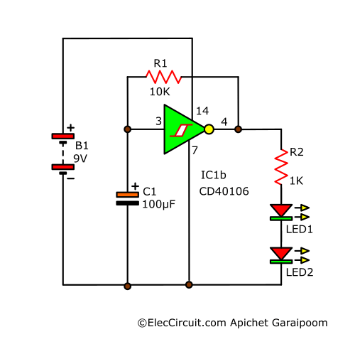
With a bit of modification of the previous circuit, we can turn it into an LED flasher circuit. First, we add LED1, LED2, and R2 into the circuit.
Then we decrease the resistance of R1 to 10kΩ and increase the capacitance of C1 to 100μF. Resulting in a very low output frequency of about 1Hz; in other words, the LEDs will flash once every second.
This circuit uses a 9V battery and a current of just 5-6mA. Also, it is recommended to use a 3mm red LED since they work at 1.7V at 3mA current. This circuit is a good foundation for an LED flasher circuit while still being very efficient.
If you are interested in an LED flasher circuit, see other LED flasher circuits on our website.
Other Circuits List
Conclusion
Using the CD40106 instead of a normal inverter gate IC is quite interesting because it functions with Schmitt trigger inputs, which is useful in certain scenarios. We are thus looking forward to using this chip more in the future, and we will be working on adding more example circuits that use the CD40106 as well.

Written by: Apichet Garaipoom
Like many others, I started electronics with curiosity and simple circuits. Over time, I’ve found joy in sharing what I’ve learned—and now, I get to build with my kids. It’s a journey, and I hope this site helps you enjoy yours.
Read more about me
Dear Apichet,
I am looking forward to all the fun circuits you design and make with your kids.
Ivor
Dear Ivor,
We appreciate your following, and we are delighted to hear that you enjoyed the content we presented.
Thank you,
Apichet
It’s refreshing to read content that doesn’t just skim the surface. You go deep, and it makes a big difference.