Last time, we talked about different types of digital logic gates. Now, let’s look at two of the most common digital ICs used today—CMOS and TTL.
We will learn about their electrical characteristics, including their input voltage and current, as well as their output.
To make it simple, we will do a simple experiment using two popular digital IC families: the SN74LS00 (TTL) and the CD4011 (CMOS).
We will learn how they work by measuring electrical characteristics with a regular multimeter. Then, compare the results with their datasheets.
The goal is to understand:
- How much current can CMOS and TTL inputs withstand?
- What load can we connect to their output?
Let’s explore it step by step—no special tools needed!
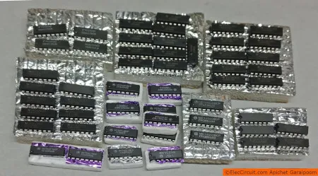
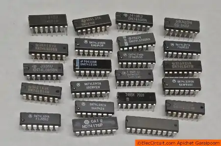
Different Digital IC Families
Digital integrated circuits (ICs) are the easiest way to use a logic gate. They come in many different logic families.
ICs from the same logic family are manufactured using the same design and technology—this often means that they cannot be used with others.
Here are digital logic families:
- Resistor-Transistor Logic (RTL)
This is one of the earliest logic families. It uses resistors and transistors, making it simple but also slow, plus it consumes a lot of power. - Diode-Transistor Logic (DTL)
This logic family uses diodes and transistors. It is faster and produces less noise than RTL. - Resistor-Diode Logic (RDL)
A basic logic family that uses resistors and diodes. It is now outdated because it is slow and not very efficient. - Transistor-Transistor Logic (TTL)
TTL used to be a very popular logic family. It uses only transistors to build logic circuits. It is faster and more stable than RTL and DTL and usually runs at only 5V. - Complementary MOS (CMOS)
CMOS is widely used in modern digital circuits. It uses both PMOS and NMOS FET transistors to build logic gates. CMOS ICs use very little power and can work over a wide range of voltages.
TTL vs CMOS
Today, most digital ICs are made using either the TTL or CMOS logic family. So, we will focus on them in particular. Each has its advantages and disadvantages.
TTL Chips – Fast but Use a Lot of Power
TTL stands for Transistor-Transistor Logic. It is also called a bipolar IC because it uses bipolar transistors.
TTL came before CMOS, so it was more common in the past and usually cheaper. With that said, both TTL and CMOS chips are easy to find online at a fair price.
They run on a 5V power supply. For the TTL chips to work properly, the supply voltage has to stay between 4.75V and 5.25V—a ±5% margin for error.
Additionally, TTL chips consume a lot of current—ranging from 8 to 100 milliamps (8–100 mA) per chip. So, if you build a project with many TTL chips—such as a microcontroller—it may need 3 to 5 amps (A) of current in total to run.
More current means more heat, so you need to watch the temperature when using them.
One good thing about TTL is speed—these chips work very fast. They can work with signals up to 30 MHz, which makes them great for high-speed circuits.
TTL inputs and outputs also behave in special ways:
- If an input is left disconnected, it reads as logic “1”
- TTL chips draw current when the input is at logic “1”
- At the output, they can sink (take in) more current than they can source (send out)
These inputs and output behaviors are different from CMOS, which we will talk about shortly.
CMOS Chips – Low Power, But Slower
CMOS stands for Complementary Metal-Oxide Semiconductor. Unlike TTL chips, CMOS uses only a type of transistor called a Field-Effect Transistor (FET). Most CMOS chips use MOSFETs, which are FETs made with a metal-oxide layer.
There are two types of MOSFETs:
• P-type (PMOS)
• N-type (NMOS)
CMOS combines both types together—that is why it is called “complementary.” This setup helps the chip use much less power. Sometimes, it is called a unipolar IC because its components—FETs—are also known as unipolar transistors.
CMOS chips can run on voltages from 3V to 16V, which is a wide range. This makes it easier to use them in different circuits.
They also use very little current, much less than TTL chips. One anecdote is that a wristwatch using a CMOS chip could last a year with just a single tiny battery. Also, since it draws less current, it doesn’t heat up as much as TTL.
CMOS chips were designed after TTL. So, they were able to improve on many of TTL’s weak points. That’s why there are many types of CMOS chips today.
However, CMOS is usually slower than TTL. Many CMOS chips work best at frequencies below 2 to 5 MHz only.
Another drawback: CMOS chips are more sensitive to static electricity. This means they can be damaged more easily than TTL chips.
Experimenting with CMOS and TTL ICs
To better understand these digital ICs, let’s do a simple experiment with them. What we are going to do includes the following:
- First, we put the chip onto a breadboard for a simpler experimentation process.
- Then, we will connect a voltage source to the chips.
- And last, we will measure how their input and output work, with a test load.
However, the operating voltages for these logic families are different. It can be summed up as follows:
- TTL requires a 5V supply voltage with a ±5% margin for error. At a 5V supply, its input “1” logic minimum voltage is 2.4V, and input “0” logic maximum voltage is 0.4V.
- CMOS accepts supply voltage ranges from 3V to 18V (B variants). At a 5V supply, its input “1” logic minimum voltage is 3.5V, and input “0” logic maximum voltage is 1.5V.
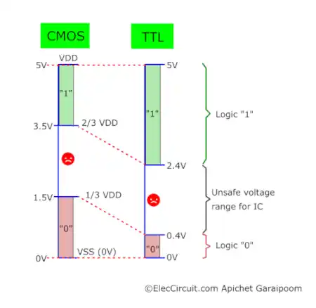
In summary, we will use a 5V supply voltage for both of these chips because that is what they accept. In addition, 5V is already a common voltage for digital circuits.
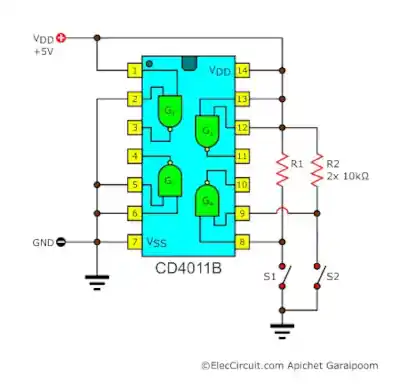
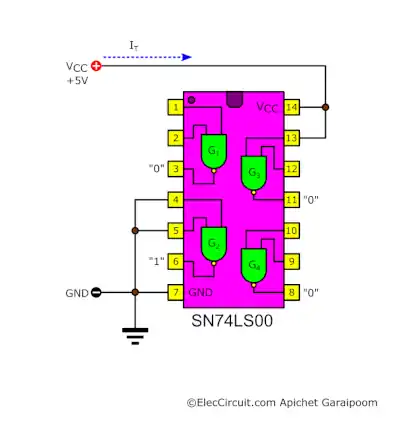
The subjects we are using today are the CD4011B for the CMOS side and the equivalent SN74LS00 for the TTL side. They both contain four two-input NAND gates.
Today, we are using the CD4011BE and SN74LS00N variants because they share the same 14-pin dual-in-line package (DIP-14). We will start with the CMOS chip and then later move on to the TTL one.
You could also do the same experiment with us. The components you would need include:
- 1 x CD4011—Nand Gate CMOS IC
- 1 x SN74LS00—Nand Gate TTL IC
- 1 x LED—Red 3mm
- 1 x LED—Red 5mm
- 1 × Resistor (1.5kΩ 0.25W)
- 1 × Resistor (330Ω 0.25W)
- Jumper wires
- Breadboard
- 5V Regulated Power Supply
- Digital or Analog Multimeter
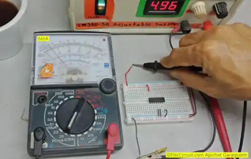
Note: In this experiment, we use a regular analog multimeter to measure voltage and current at the input and output of both chips.
Although this meter is quite old (over 20 years) and harder to read than a digital multimeter, it still works well. Right now, we have to use it because the other meters are broken.
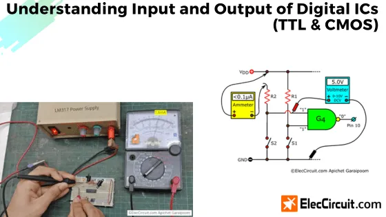
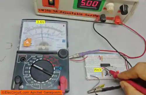
CMOS NAND Gate
As we said before, the CD4011B chip contains four different NAND gates. Each gate has two inputs and a single output. These input and output pins match the pin numbers of the IC.
For example, gate 1 (G1) uses pins 1 and 2 for its inputs and pin 3 for its output.
Next, we will call the four gates G1, G2, G3, and G4, as shown in the diagram below.
After we finish putting the circuit together like the layout above, we check if any wires are connected wrong. Then, we connect a 5V power supply to the circuit. In this circuit, 5V means logic “1”, and 0V means logic “0”.
Now, we want to check that the NAND gates are working as they should.
You might see that G1, G2, G3, and G4 have different inputs.
If that’s hard to see, we can show each logic gate one by one, like in the diagram below.
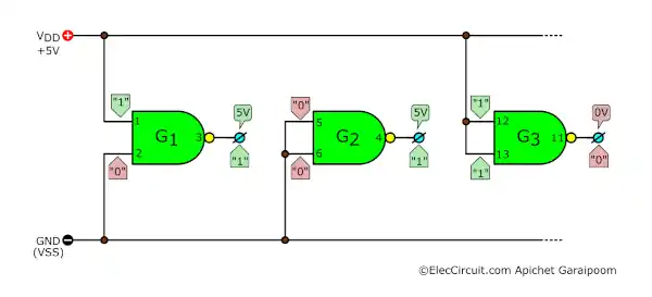
We use a voltmeter to measure the output voltage (at pins 3, 4, and 10) of the first three gates, relative to ground (GND). By “measure,” we compare the output voltage to ground.
Here is a summary of each gate’s inputs and outputs:
- G1 receives “1” and “0” as logic inputs → outputs “1” (5V)
- G2 receives “0” and “1” as logic inputs → outputs “1” (5V)
- G3 receives “1” and “1” as logic inputs → outputs “0” (0V)
These input-output values match exactly with a truth table for a NAND logic gate.
Inputs Behavior
The G4 is different, however, as we connected two 10kΩ resistors from the VDD to its inputs. Generally, CMOS chips have a very high input impedance. Thus, even with the resistor, the G4 inputs should still receive 5V, or the “1” logic level.
We are seeing a logic “0” at the output (pin 10) because both switches are turned off (not connected / open).
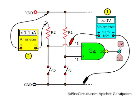
We also measure the voltage at the G4 inputs (pins 8 and 9). The resulting voltage is 5V, as expected.
Next, we set the meter to ammeter mode and measure how much current flows through the resistors from VDD to the input. This tells us how much current the gate pulls when idle.
The result is less than 0.1μA—too little to affect anything in most cases. If any CMOS chips pull more current than this, they are likely malfunctioning.
Next, what will happen if we turn on switches S1 and S2? Let’s find out.
The CMOS input draws almost no current, so the current flows through the switches instead. They act as the easiest path to GND.
As a result, the voltage at both inputs changes from 5V to 0V. Their logic also changes from “1” to “0.”
Switches like this make it easy to change the input between “1” and “0” without moving any wires.
Outputs Behavior
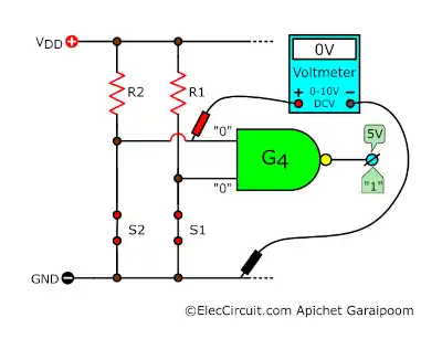
In a CMOS chip, logic “1” is 5 volts (supply voltage), and logic “0” is 0 volts. This is true when nothing is connected to the output.
Let’s set S2 to off and S1 to on. Now, G4 gets a ‘1’ and a ‘0’ as inputs. So, it outputs a ‘1’ (5V).
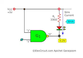
To measure the output current, connect a load to the output. This load includes a current-limiting resistor and an LED, as shown below.
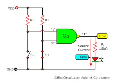
Electric current flows from the output pin to ground. This current turns on the LED. This type of current is called ‘source current’ or ‘drive current.’
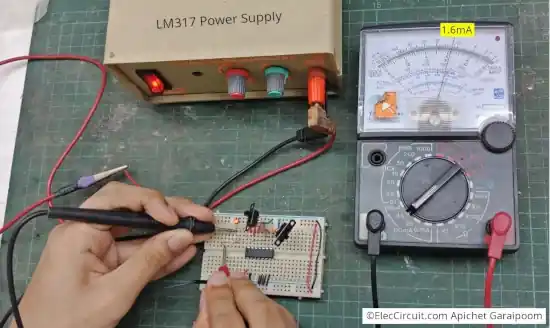
When the output is high, current flows out of the IC. In our test, the source current was about 1.6mA at 4.6V.
The CD4011 datasheet, the typical source current is -1mA when the output voltage is 4.6V and the supply is 5V.
The current is shown as negative because of how it was measured: the ammeter’s negative probe was connected to the output, and the positive probe was connected to GND.
Now turn off both switches to disconnect the inputs. This makes both NAND gate inputs high, so the output goes low (0V). Since the output is now at ground, we need to reverse the resistor and LED to allow current to flow, as shown below.
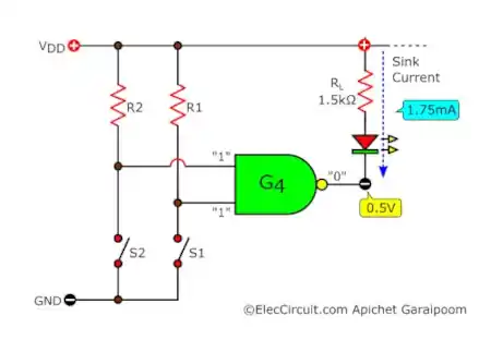
When the output is low (logic “0”), current flows from VDD through the LED and into the output pin. This is called sink current. In this case, the chip pulls current into itself.
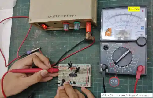
We measured the sink current to be about 1.75 mA at an output voltage of 0.5 V. This is higher than the source current measured earlier.
Like the source current, the datasheet tells the sink current at a 5V supply is 1mA at a 0.4V output voltage.
TTL NAND Gate
Next, we’ll test a TTL chip. For this experiment, we are using the SN74LS00, which contains four two-input NAND gates—just like the CD4011B. Although CMOS and TTL chips are built differently, the logic of their NAND gates is the same.
We will start by putting the SN74LS00 into a breadboard. Then, connect a 5V power supply and GND to pins 14 and 7, respectively.
Notice that the SN74LS00 has the same 14-pin package as the CD4011B CMOS chip. However, the pin functions are arranged differently. Pins 3, 6, 8, and 11 are outputs. The other pins are inputs, except for pin 14, which is VCC, and pin 7, which is GND.
No-load total current
This time, we also measure the no-load total current with an ammeter; the result is about 6mA. In the case of the CMOS chip, the input current is almost zero.
Disconnected inputs
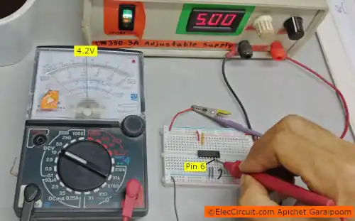
We then measure the output voltage at pin 3 (G1). The result we get is 0.1V, which indicates a “0” logic level.
A NAND gate outputs “0” only when both of its inputs get “1” logic, meaning that TTL inputs get “1” when they are unconnected (floating), because none of the G1 inputs are connected.
Even so, we measure the voltage at the inputs (pins 1 and 2) with respect to the GND. The voltmeter reading shows 1.5V, which falls outside both the “1” and “0” logic voltage ranges.
According to the SN74LS00’s datasheet, the “1” logic level input voltage must be higher than 2V, and the “0” logic level input voltage must be lower than 0.8V.
Notice that the 1.6V is not within both ranges. So, it is not recommended to leave the input pins of TTL chips disconnected.
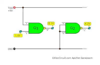
When no load is connected, TTL and CMOS differ in their output voltages. For example, the SN74LS00 gave 4.2 V for logic “1” and 0.1 V for logic “0”.
Inputs Behavior
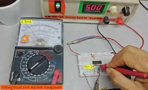
Next, let’s look at the TTL input behavior. We’re using gate G1, with pin 1 (one input) connected to VDD (the positive supply) and pin 2 (the other input) connected to GND. Then, we measured the current flowing into or out of both inputs.
At pin 1, which gets logic ‘1’, a small current flows into the gate. We measured this input current at about 50 μA.
On the other hand, at pin 2 (logic ‘0’). We measure a current of about 0.5 mA, higher than the 50 μA we measured at pin 1.
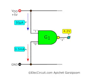
Compared to the CMOS chip, its input draws almost no current — even when connected to VDD or GND. This is a clear difference from TTL.
Outputs Behavior
For the output behavior, we’ll begin with the source current, then move on to the sink current. Along the way, we’ll also check the output voltage.
The Source Current
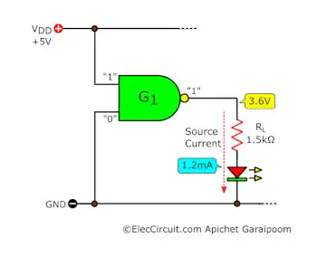
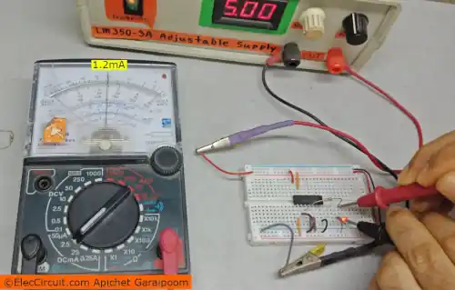
To test the source current (logic “1”), we used the same load as in the CMOS test: a 1.5 kΩ resistor (RL) and a 3 mm red LED.
With this setup, we measured the TTL output source current at about 1.2 mA, which is less than the CMOS chip. Why is that?
To find out, we also measured the output voltage. It dropped from 4.2 V (no load) to just 3.6 V with the load. According to Ohm’s Law, if the resistance stays the same (1.5 kΩ), a lower voltage results in a lower current.
From the SN74LS00 datasheet:
- The source current is about 0.4mA (chip sends out this much current)
- Logic “1”, the voltage should be 2.4V or higher.
- Logic “0”, the voltage should be below 0.4V.
Now, let’s test the chip when it outputs logic “0” (sink current).
From the datasheet, the chip can sink up to 8mA of current safely.
We change RL to 330 ohms. We also swap the LED for a 5mm one (bigger than the 3mm). Bigger LEDs are usually brighter and need more current.
After that, we measure the sink current.
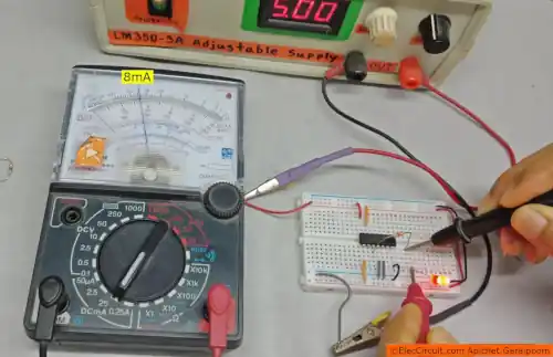
The sink current we measured is 8mA, just like the datasheet says. The output voltage also rises a little—from 0.1V (no load) to about 0.2V. That’s still under the 0.4V limit for logic “0”.
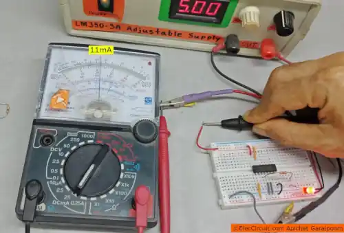
Next, we tested the total current again. The current rises to 11 mA. The load uses more current — that’s why the total current is higher.
Fix the low current
From these tests, we saw that the output current from both CMOS and TTL is quite low.
So in real circuits, we fix this using simple methods:
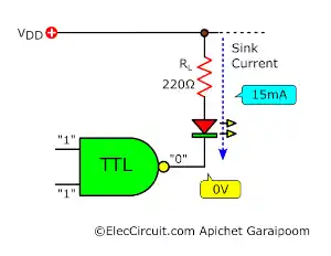
1. Use sink current to drive more current. For example, as shown below, we can use a 220-ohm resistor (RL) with an LED. This can drive up to about 15mA.
2. Use a transistor to help.
In source current mode, we can add a small transistor (like the 2N3904). This boosts the current enough to light the LED.
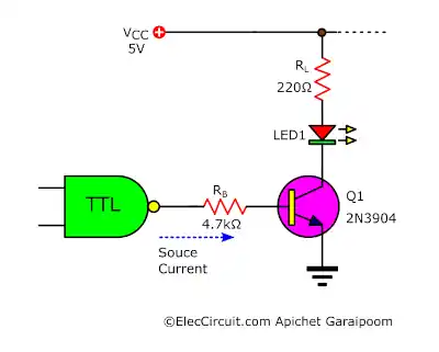
This also lets us change the load to other components that need more current—like a buzzer, relay, and so on. But we still need to calculate the base resistor (Rb). We’ll show some examples next.
Our member area also contains this content.
You can download it in PDF format with larger images, while the content remains the same.
I appreciate your support.

Written by: Apichet Garaipoom
Like many others, I started electronics with curiosity and simple circuits. Over time, I’ve found joy in sharing what I’ve learned—and now, I get to build with my kids. It’s a journey, and I hope this site helps you enjoy yours.
Read more about me