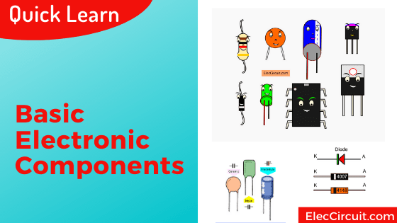
Let me tell you about the basic electronic components list with images. If without knowing the name and how they work, then we cannot use them to build electronic circuits. That includes resistors, capacitors, diodes, transistors, LEDs, integrated circuits(ICs), etc.
Most components have two or more terminals(lead or pins). To solder them on the circuit boards or wire connection.
On this page is an overview of basic electronic components. You can get in-depth information by clicking on the link of each component.
Here are 10 Components below!
1# Resistors—resist the flow of electricity
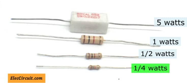
Mostly we use the resistors to divide a voltage into a smaller voltage. This makes them very useful for reducing the current going to light-emitting diodes or other loads, that can be damaged by too much current.
Resistors are also used to increase the time required to charge capacitors and speed up the discharge of capacitors.
And, they are used to control the gain of amplifiers.
Read more:
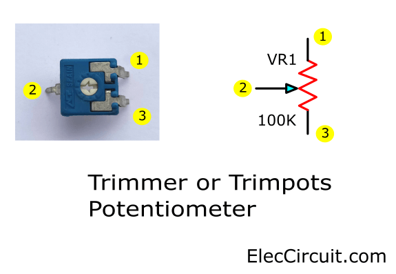
Trimmer Potentiometer
It is a type of variable resistor. Some called it the trimpots. We can adjust its resistance. See below.
2# Capacitors—store an electrical charge
They have many uses. For example
- Store an electrical charge
- To smooth a fluctuating Signal
- Block continuous current while passing current pulses
Read Also
- Capacitor Principle working, types, and how it works
- Uses of capacitors | RC circuit time constant and Coupling
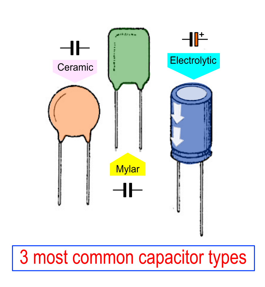
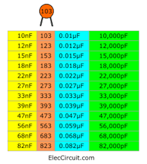
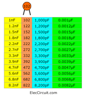
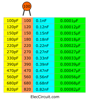
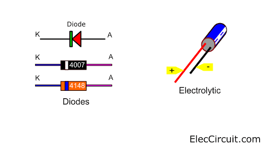
Capacitors have many types and sizes. We often use these three types of capacitors: Ceramic, Mylar, and Electrolytic.
- The Electrolytic has a lot of capacitance shown on its body.
Importance! It is a polarised capacitor, therefore it has a positive and negative lead.
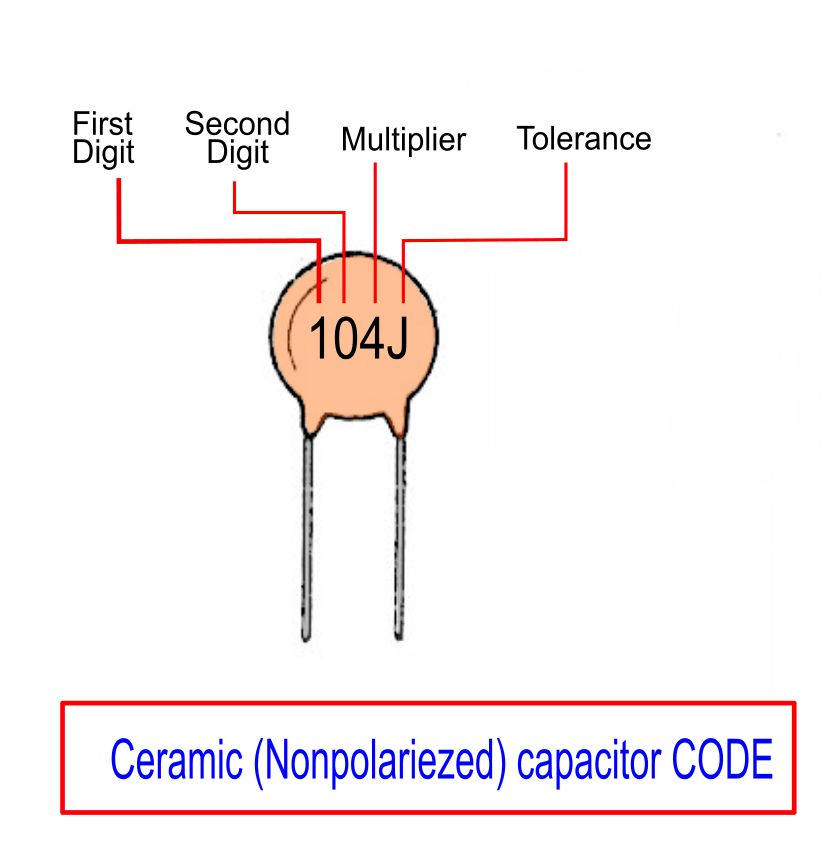
Its negative lead (have a mark on it and a shorter lead) must always connect to the negative voltage. - The Ceramic and Mylar have less capacitance than the Electrolytic. They are often very small compare to the Electrolytic ones. Therefore, there is a capacitance code on them instead.
Capacitance code calculator:
For example, 104J is 0.1μF on 5% tolerance.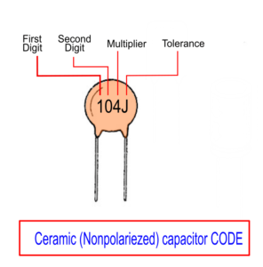
- First and Second Digit are fixed numbers, both numbers tell units in pF
- The third digit is multiplied by the number of the power of ten.
For example 104 = 10,000 - Fourth is tolerance level such as J = 5%, K = 10%, M = 20%.
How to do it
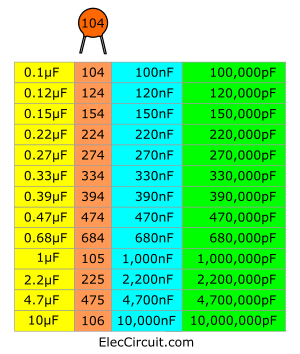
What is the 104K capacitor value?
10pF — First and Second Digit
10pF x 104 = 100,000 pF. Which is 0.1μF and 10% tolerance.
Capacitors list
But deciphering the above might be too complicated. So my daughter put together a list of capacitors that we had seen:
3# Diodes—one-way valves for electrical current
The diode functions as a rectifier, allowing the current to flow one way. It must be connected in a proper way.
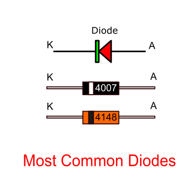
Diodes have different sizes and usage according to their spec. Their number will be printed on its body. As illustrated above is a diode that we often use.
4# LED—great light sources
Now a day, almost all the light sources, we often choose to use LED. Because they have better efficiency. They also have lower power consumption, long lifetimes, and many colors.
But, what we should know:
- LED is the Light-Emitting Diode.
- It works when gets a forward-bias voltage across it and the voltage must exceed a threshold level of about 1.8V and the current of about 10mA up.
- Do not use the voltage higher than 2V (depending on the type of LED). Because it will heat up and causes damage to itself.
- Must be connected in a correct polarity, the LED will glow. But if connected in the wrong polarity (reverse bias), it will be no current flow through.
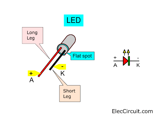
As illustrated above, a flat spot on the rim at the base of the LED. It will indicate the negative (-) or cathode (K). Or if the LED is brand new, the short leg will always be K.
5# Zener Diodes—keep a fixed voltage across them
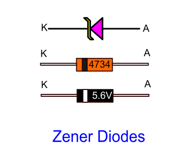
They have a shape like a diode, and they also work similarly. A positive current can pass through the anode to the cathode easily.
Normally, this current will be unable to flow backward through the cathode to the anode. But if the voltage drops across it go up the set-point voltage, it will allow this current to pass. This voltage is called a Zener diode voltage (VZ), and it will not change.
For example, VZ is 5.6V. Therefore, we often use it as a constant voltage regulator.
Read More: Zener Diode: How to use, example circuit usage
6# Transistors—make an amplifier or switching circuit
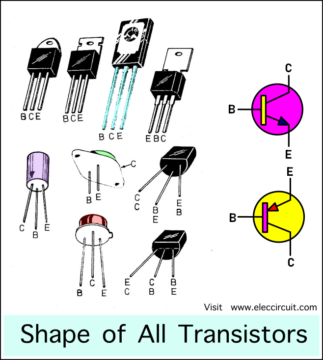
Transistors are semiconductor devices with three leads. Usually, a very small amount of current at the B lead can control a much larger amount of current flowing through the C to E leads.
All transistors can be put into two main groups. The first group is the NPN type, almost everyone prefers this type because it works in positive voltage. The other group is PNP types, they work in the negative.
Transistors have many different shapes, according to usage characteristics. Its number will be printed on its body.
Recommended:
- How does a transistor work and used
- Experiment with transistor as switch
- Experiment with Parallel Transistors for More Current
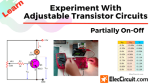
- Experiment with adjustable transistor circuits partially on-off
- Learn: Designing small signal amplifier circuit using transistor simply
Look at transistors that we use often.
My daughter often has problems with these tiny transistors because they look the same. But the position of their legs is different. It may cause the circuit to malfunction or be damaged. Therefore, we must always pay attention to its number.
7# SCRs—Silicon-Controlled-Rectifiers
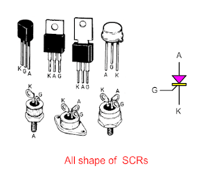
The SCR is similar to a bipolar transistor. But its symbol is similar to a diode with having three legs.
It acts as a barrier to prevent electricity from flowing through the Anode (A) to the Cathode (K). Until there is a control current to trigger the Gate (G).
But electricity can not flow backward from the Cathode to Anode.
They have the symbol and shape as the above picture.
Read more: How SCR works and using
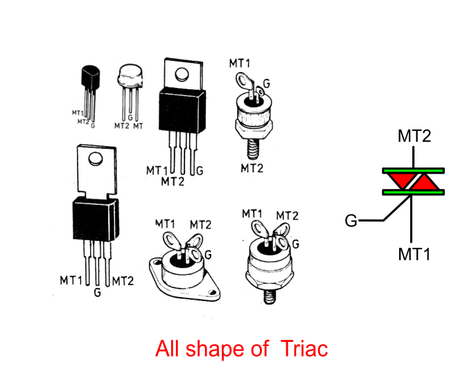
7# Triac—two SCRs connected in parallel
Triac acts similar to an SCR. But it allows both directions of currents to flow through MT1 and MT2 if it has proper current control through Gate (G).
Therefore, they are good at an AC switching controller. They have symbols and shapes as illustrated below.
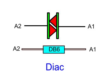
8# Diac—similar to Zener diode in parallel
The Diac is similar to a Zener Diode. Usually, it will not allow the current to flow through both sides. Until the voltage drops across it, reaching the specified value only.
Here are the shapes and symbols.
9# ICs—Integrated Circuits
IC stands for the Integrated circuit. The IC is an electronic device with integrated circuits inside it, with many legs coming out to be used.
We need to read a variety of functions in the manual of that specific IC. The most common models are the Dual In the Package (DIP).
The IC has a pin counting system as follows:
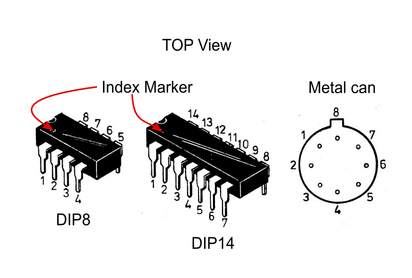
Look at it from the top of the IC. You will see an index marker to indicate pin 1. Then, we start to count counterclockwise from the first pin close to the index point. The number of each IC is printed on the chassis as shown.
On right is a metal can model, usually an OP-AMP IC. It is a high-quality model, but expensive.
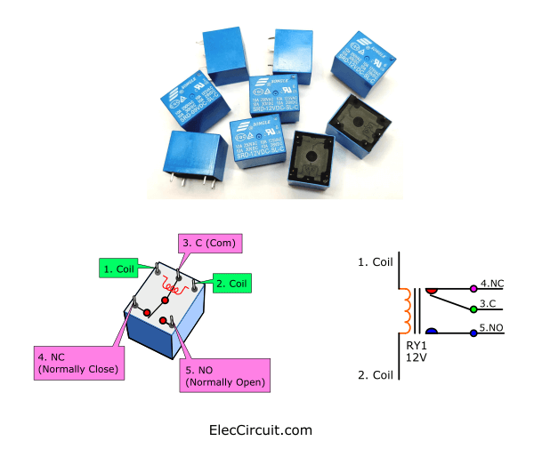
10# Relay
A relay is an electromagnetic switch. Though they are very ancient, they still have many uses. They are controlled by a low voltage or small current, which switches a larger or higher current to others. A small current flowing through a coil in the relay creates a magnetic field that pulls one switch contact against or away from another. We like to use SPDT contacts relay as a symbol and connection in illustration.
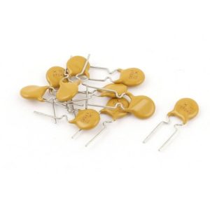
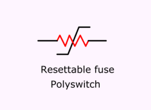
11# Resettable fuse or Poly Switch
Have you ever used a fuse? It protects any parts from the excess current. He (fuse) will sacrifice himself by having a high current blow it away. This component has been called by many names: Resettable fuse; Poly switch; Multi fuse; Polyfuse. They are all passive electronic components and function similarly to PTC thermistors.
There are many sizes to protect against the current. Such as 0.4A 75V, 72V 500mA , etc.
Look:
Cr: by uxcell
It looks like capacitors but it is a great fuse.
And see a poly switch symbol.
What is the device that I have problems with the most?
It is Diodes and Electrolytic capacitors.
Not only that you should learn:
Related Posts


I love electronics. I have been learning about them through creating simple electronic circuits or small projects. And now I am also having my children do the same. Nevertheless, I hope you found the experiences we shared on this site useful and fulfilling.
Very Important To Learn!!!!
Hi, Friend!
How are you?
Thanks for your feedback.
Hi Is the Book “Basic Electronic Components” available and from where and the cost, please.
Regards.
AlanBB.
Hi Alan Brett-Brazill,
Thanks for your feedback.
I am not sure where sell that book and cost.
Shut it down the doorbell
Great lesson
Hi,
Thanks for your feedback. It’s my pleasure. 🙂
well explained the parts.
Hello Peter Kiluye,
Thanks for your feedback.
I am the mobile technician
Hello, Suresh badditi,
Thanks for your visit. I am happy that you comment.
Please tell me what do you want?
Thanks
Hi, thanks for your presentation and quick learning on electronics
You are welcome, My friend!
Your lecture is supper, thank you.
Please can you send me PDF of this lecture in my mail?
If yes i will so much appriciate .
ezekielokekanyin@_gmail.com
Currently, I am still increasing more content to it. I will send it to you when it is done. Please be patient.
Good Day,
I am very happy to see this subject thanks a Loat,
dear I am very new in this subject. I am basically from HVAC side. But I NEED TO LERN ELECTRONIC TOO I NEED UR SUPPORT
Good day, too.
Thanks, It is great. Are you an HVAC engineer? I’m going to build a house in the garden by myself.
It is great for us to share our experiences with each other. I have a passion and aptitude for simple electronics to teach my kids and share with friends on this website.
I love your site I need video of the spar parts how its worked i wans see the like demo
Indactr coil, capacitar, diode, risister, and transistor 5 componts full ditels pdf send mi sir 🙏🙏🙏🙏
Hi,
Currently, we do not have a detailed version in pdf format.
U are the best thank you very much for knowledge
Thank you very much for your encouragement.
We are encouraged to continue writing articles. 🙂