

Crossover distortion is one of the major limitations of a basic class B push-pull amplifier. Near the 0V crossing point, neither the NPN nor the PNP transistor conducts fully, causing a small discontinuity to appear in the output waveform.
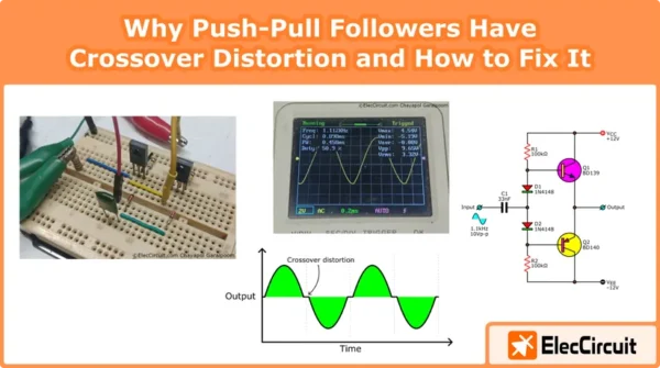
In practical amplifier circuits, this distortion is usually reduced by adding a biasing network between the complementary transistors. Doing so shifts the push-pull stage from class B operation to class AB operation, improving waveform continuity and reducing distortion.
In this article, we’ll look at why crossover distortion happens in a push-pull follower circuit and how a simple transistor bias network can reduce it. We’ll also examine a simple pre-drive stage used to offset the voltage drop.
Reviewing the Class B Push-Pull Stage
In the previous part, we built and tested a basic class B push-pull follower using complementary BD139 and BD140 transistors without any biasing network between them. Just a basic circuit with a simple coupling capacitor at the input, as shown in Figure 1.
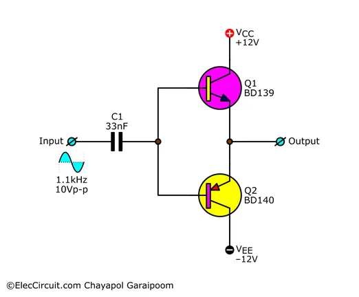
However, when loaded, the output signal shows signs of discontinuity or “notch” between the positive and negative halves of the waveform. This discontinuity is caused by crossover distortion.
So, in this article, we’ll look for a way to remove this distortion from a push-pull follower circuit. But first, let’s learn more about crossover distortion and its causes.
What Is Crossover Distortion?
Crossover distortion is a prominent problem in class B complementary designs, such as in a push-pull follower circuit. It occurs when the input voltage falls between the turn-on thresholds of both transistors—typically between about +0.65V and –0.65V.
Within this voltage range, the conducting transistor is turning off, while the other has not yet turned on. As a result, neither transistor conducts a meaningful amount of current. This is sometimes called a “dead zone.”

This creates a small discontinuity (or “notch”) between the positive and negative halves of the output waveform. As we saw with the circuit in Figure 1, this effect becomes a lot more noticeable when driving a low-resistance load.
There are various ways to reduce the effect of crossover distortion. A common solution is to add a biasing network that slightly turns on both transistors even at 0V input.
This shifts the operation of the push-pull follower from class B to class AB, where the conduction of the two transistors overlaps slightly, smoothing out the transition.
Other approaches include applying negative feedback, such as with a differential amplifier stage, which further reduces distortion. This idea is also quite intriguing, so let’s put a pin in it for now.
Improved Push-Pull Circuit Designs
Now that we know what it is, let’s look for ways to reduce the crossover distortion from our push-pull stage. In this section, we’ll explore various iterations and improvements to the push-pull follower design until we reach a circuit we think is good enough for our use.
Resistor-Diode Bias Networks
Starting with a simple bias network consisting of RB resistors and diodes for the two transistors. The circuit schematic of this improved version is shown in Figure 3.
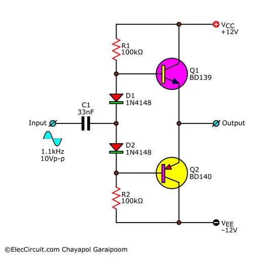
D1 and D2 are 1N4148 switching diodes with a relatively constant forward-bias voltage drop. R1 and R2 set the bias current through the diodes, ensuring they remain forward-biased and establish a voltage drop of approximately 0.6V-0.7V each. C1 is a coupling capacitor.
How The Bias Network Works
How it works is rather simple. When powered, current flows from VDD through R1, D1, D2, and R2, down to VEE. This creates a voltage drop across all four components.
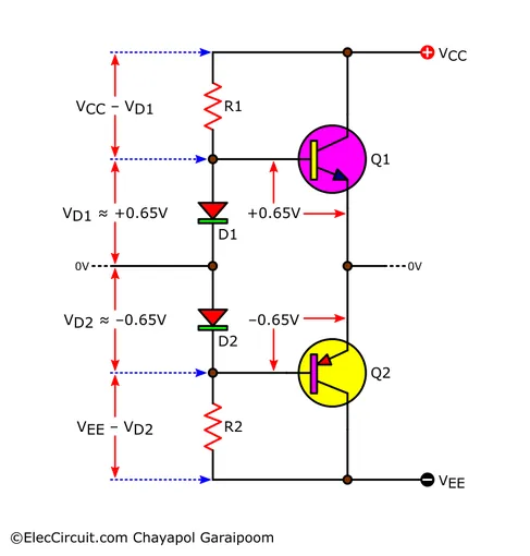
However, the voltage drop across D1 and D2 is much lower than the resistors because of their low forward-base resistance. Ideally, we want the voltage across the diodes to follow the transistors’ VBE, which is about 0.6V to 0.7V.
This ensures the base voltage of Q1 is about VBE higher relative to the input, and Q2 is about VBE lower. As a result, both transistors conduct slightly at 0V input, eliminating the “dead zone” in conductivity.
Another way to look at it is that the diode pair establishes fixed voltage offsets of approximately +0.65V and –0.65V relative to the input. They behave somewhat like a normal resistive voltage divider, although the diodes act almost as constant-voltage components rather than simple resistors.
As the positive and negative supply rails have equal but opposite potentials, the resistor-diode bias network is symmetrical for both Q1 and Q2.
Testing The Improved Bias Network
Next, we try this improved version out on a breadboard. R1 and R2 are 100kΩ, same as in the schematic. These values provide sufficient bias current through the diodes while minimally loading the previous stage.
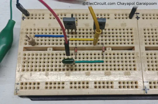
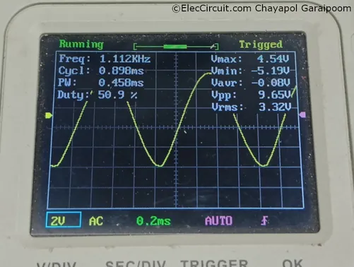
When driven with the same 10Vp-p 1.1kHz sine signal, the resulting signal reading shows a 9.65Vp-p, shown in Figure 3.4. This is notably higher than the 9.08Vp-p observed in the version without a bias network.
Then we add the same 560Ω resistor load to the output (Figure 3.5).
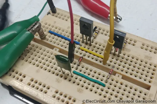
With the load present, the output peak-to-peak voltage drops slightly to 8.84Vp-p. More importantly, the waveform shows no visible discontinuity at the 0V crossing, showing that the crossover distortion has been effectively reduced, as shown in Figure 3.6.
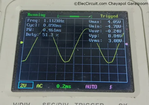
We do still see a slight clipping at the negative peak, however. This asymmetrical clipping is likely because of limited negative-voltage swing and insufficient base drive for the PNP transistor (Q2) under load.
That said, fixing or reducing this clipping effect is also pretty easy with another pre-driver stage, as we’ll see in the later version.
All in all, this biasing method proves effective and simple to implement, while still significantly reducing crossover distortion and improving the push-pull stage’s voltage swing.
Adding a Pre-Driver Stage
Even though the previous improved circuit works quite well, there are a couple of drawbacks. These drawbacks include a noticeable output voltage drop when driving a load and slight clipping in the negative cycle.
To address these concerns, we can add a pre-driver stage before the push-pull follower stage. This stage provides additional voltage gain and base drive, allowing the push-pull stage to achieve a wider, less limited output voltage swing.
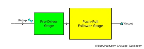
The pre-driver stage is typically a common-emitter amplifier, where a transistor controls the current flowing into the bias network of the push-pull stage.
So, let’s add to the push-pull follower a simple CE amplifier pre-driver stage along with a voltage divider to limit the effective voltage gain, as shown in Figure 5.1.

How The Pre-Driver Stage Works
R1 and R2 form a bias network that sets the base voltage of the pre-driver transistor Q1, while VR1 allows fine adjustment of this voltage.
The capacitor C2 is placed between the base and collector of Q1 and acts as a compensation capacitor, reducing high-frequency gain and preventing oscillation between stages.
Q1 is effectively controlling the current flowing into the push-pull stage. Meanwhile, R3 and R4 function both as bias resistors for the push-pull stage and as the collector and emitter resistors for Q1. As a result, the pre-driver and push-pull stages are tightly integrated, sharing both biasing and load paths.
In the schematic shown in Figure 5.1, the input signal enters via the top of the voltage divider (VR2 and R5) and is then coupled to the pre-driver stage with the coupling capacitor C1.
In this configuration, the voltage divider output depends on the ratio between VR2 and R5. When VR2 is exactly 0Ω, the ratio becomes 1, and the full input signal appears at the output. When VR2 is at 1MΩ, the output is reduced to approximately:
$$V_{out} \approx V_{in} \times \frac{180k\Omega}{1M\Omega + 180k\Omega} \approx V_{in} \times 0.15$$
For a 10Vp-p input, the possible output of this divider network ranges from approximately 1.5Vp-p to 10Vp-p.
Testing Pre-Driver Version
Next, we assemble this version of the circuit onto a breadboard, as shown in Figure 5.2.
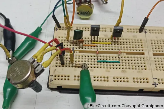
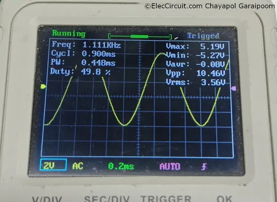
We can adjust the input amplitude freely (as long as it’s within the range) using VR2. After a quick adjustment to VR2, the output waveform closely follows the input signal, producing a clean 10Vp-p output with no visible crossover distortion or clipping.
One small drawback with this voltage divider design is that its minimum output value is slightly above 0V—about 1.5Vp-p according to the calculation.
In other words, we cannot completely turn off the signal by just adjusting VR2 alone; there will always be some signal at the circuit’s output as long as an input is applied.
Why don’t we use one potentiometer as a voltage divider? We discussed more about the downside of that approach in the more in-depth version of this article. See below if you’re interested.
Conclusion
While these improvements to the push-pull follower circuit work relatively well, there are still some drawbacks worth mentioning.
For instance, because the pre-driver stage has a fixed voltage gain, every time the input amplitude changes, we would have to manually correct it using the voltage divider at the input. The output signal also isn’t the most stable.
Hence, in practical audio amplifiers, the push-pull stage is typically combined with a negative feedback stage, such as a differential amplifier, to stabilize the operating point and improve performance.
Want to learn more?
We’ve extended the topic covered by this article on Patreon (70 pages, 7642 words) with extra content, including more experiment notes, practical testing, observed drawbacks, circuit improvements, and more.
👉 Read complete transistor push-pull follower on PatreonExclusive posts on Patreon come free of advertisements and in PDF format with high-definition illustrations. Membership fees will allow us to continue to do what we do without as much reliance on advertisement. Thank you very much.
Hello. I’m Chayapol, but I could also go by Aot. I write and draw illustrations for ElecCircuit.com.
I usually cover articles related to digital electronics, logic, or basic principles or ideas on the site.