
A push-pull follower is one of the most common transistor output stages used in audio amplifiers and other power amplifier circuits. By using complementary NPN and PNP transistors, the circuit can source and sink current efficiently while allowing the output to swing around 0V.

A single-ended emitter-follower output stage has a DC-biased output and requires a coupling capacitor to drive a load properly. A push-pull follower solves this problem while also improving output power and efficiency.
In this article, we’ll look at how a basic transistor (BJT) push-pull follower works, how it behaves under load, and some of the limitations we found in real-world usage.
What Is a Push-Pull Follower?
A push-pull follower is a transistor power amplifier that uses a complementary pair of NPN and PNP transistors to drive a load. It’s also known as a complementary symmetry amplifier because of how the two transistors are arranged.

In this configuration, the two transistors conduct alternately, sourcing and sinking current from the positive and negative supply rails. As a result, a push-pull follower requires both positive and negative voltages to function.
Compared to a single-ended emitter follower stage, it generally offers high output power and better efficiency. More importantly, a push-pull follower’s output swings around the 0V midpoint with no DC offset, allowing it to drive a load directly without a coupling capacitor.
At the same time, the push-pull design still provides equal or greater current-driving capability compared to the single-ended emitter follower stage, a feature we still need.
That said, a push-pull follower is susceptible to a specific type of distortion that appears at the point where one transistor turns off, and the other turns on. This is known as crossover distortion, which we’ll explore in more detail later.
Why Use a Push-Pull Follower?
In the previous article, we built a simple transistor amplifier using a common-emitter stage followed by an emitter follower output stage. It performs rather well, providing reasonable voltage gain along with a significant current boost from the emitter follower.
However, the main limitation with the emitter follower is that the output is DC-biased. Because of its single-ended design, the output sits roughly at the midpoint of the positive supply when the input is 0V and swings up and down from there. As a result, we need a coupling capacitor to connect it to the load, which decreases the output power.
On the other hand, a push-pull follower outputs a signal centered around a 0V midpoint (no DC offset), eliminating the need for a coupling capacitor and allowing for a smaller circuit.
In addition, the push-pull design improves efficiency by allowing each transistor to conduct only half of the waveform. This enables greater output power and stronger load-driving capability compared to a single-ended follower stage.
How Push-Pull Follower Works
For this explanation, we’re using a sine-wave signal as input and an RLoad resistor functioning as a load.
Let’s begin with the signal’s positive half-cycle. During this phase, the input voltage rises, driving base current into the Q1 NPN transistor while Q2 remains off.
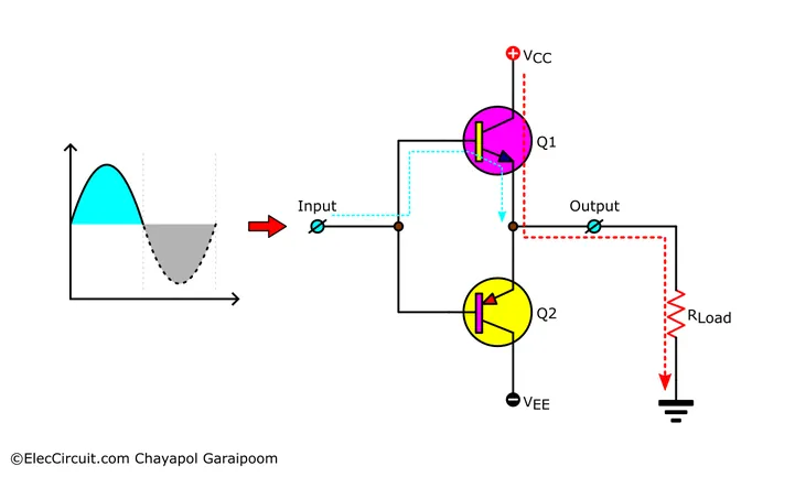
This causes Q1 to conduct current from VCC (positive supply) into RLoad. In other words, Q1 is currently sourcing current to the load.
During the negative half-cycle of the input sine signal, the input voltage falls. As a result, base current flows through the Q2 PNP transistor, turning it on while Q1 turns off.

Q2 then starts to conduct current from RLoad to VEE (negative supply). In this case, we can say that Q2 is sinking current from the load.
Because both Q1 and Q2 conduct current during the opposite halves of the input signal, they each produce one half of the output waveform—Q1 produces the positive half swing, while Q2 produces the negative half swing, as shown in Figure 4.3.
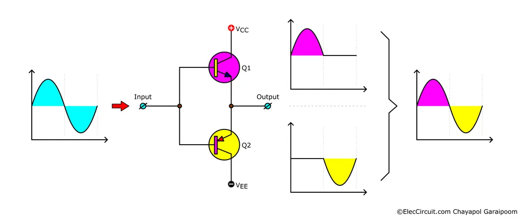
At the output, these two halves are recombined, producing a signal that closely follows the input waveform.
For this to work seamlessly, the two transistors must have as similar characteristics as possible. Otherwise, the difference between them will introduce distortion to the resulting signal.
In the case of no input, both Q1 and Q2 go unbiased, thus producing 0V at the output.
Additionally, since the two transistors take turns conducting, a push-pull follower usually operates as a class B amplifier (or class AB in practical designs we’ll run into later).
Simple Test of the Initial Push-Pull Follower Circuit
To find out if this circuit could work in practice, we figured the best way was to test it with real components.
The transistors we’ll be using are a pair of BD139 NPN and BD140 PNP. These two audio transistors are designed for complementary operation, making them ideal for this circuit. They’re connected as a push-pull circuit, shown in Figure 3.1, which follows the same basic configuration introduced earlier.
For the power supply, we’re using +12V/–12V for VCC and VEE, respectively. Additionally, we add a 33nF input coupling capacitor at the input to connect to previous stages.
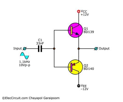
The input for this test is a 1.1kHz 10Vp-p sine wave signal. We decided to carry out this test on a breadboard, as it allows for easy adjustment and is easy to put together as a whole. The circuit is also very basic, as shown in Figure 3.2.
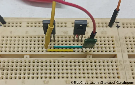
Now, let’s hook up the input signal to see what will happen.

The output voltage drops approximately 1V to 9.08Vp-p compared to the input (10Vp-p input vs. 9.08Vp-p output). Mind you, this figure is without any load. So why does the voltage drop?
This is mainly because of the voltage required to turn on each transistor. During each half-cycle, the conducting transistor introduces a voltage drop of about 0.6V-0.7V. Because this occurs on both the positive and negative halves of the waveform, it could reasonably take about 1Vp-p away from the overall output.
Note that something similar also happens with a single-ended emitter follower, where the output follows the input minus the base-emitter voltage (Vout ≈ Vin – Vbe). This drop can be offset, however. But we’ll have to save that for later.
Try Adding a Load
Of course, without a load, it doesn’t prove anything to us. So let’s add one. We decided not to go too overboard and started with a 560Ω resistor load for the time being.
With the 560Ω load, the output peak-to-peak voltage drops to about 8.68Vp-p while the waveform still looks sine-ish.

However, notice that near the 0V midpoint, there is a slight “notch” between the positive and negative halves of the waveform. This happens because neither Q1 nor Q2 conducts fully near the 0V midpoint region, thus producing minimal output.
This is known as “crossover distortion“ and is one of the main limitations of the basic class B push-pull stage like the one we’re working with here. In the next part, we’ll look at how we can reduce this distortion using bias networks used by many practical circuits.
Want to learn more?
We’ve extended the topic covered by this article on Patreon (70 pages, 7642 words) with extra content, including more experiment notes, practical testing, observed drawbacks, circuit improvements, and more.
👉 Read complete transistor push-pull follower on PatreonExclusive posts on Patreon come free of advertisements and in PDF format with high-definition illustrations. Membership fees will allow us to continue to do what we do without as much reliance on advertisement. Thank you very much.
Hello. I’m Chayapol, but I could also go by Aot. I write and draw illustrations for ElecCircuit.com.
I usually cover articles related to digital electronics, logic, or basic principles or ideas on the site.