
What is a gated SR latch—also known as a clocked SR flip-flop—and how do they work? In this article, we learn how they work and their differences from a normal SR latch.

Here is a short recap on what an SR latch is. It is a type of sequential logic with at least two inputs — Set and Reset. The Set input sets the output to logical “1,” whereas the Reset input sets the output to “0.”
You can learn more about the SR latch in our in-depth article on the subject here: How an SR Latch Works – A Step-by-Step Guide
Now that we have a basic understanding of how an SR latch works, let’s look at what the ‘gated’ part of the gated SR latch very means.
Gated or Pseudo-Transparent Inputs
Normal logics, like SR latches, are transparent logical components. This is because when we apply the input, the output changes immediately. Meaning the input is always enabled.
On the other hand, non-transparent components will not change their output after we apply the input if a certain condition is not met. In other words, its input is disabled when the condition is not met.
This is not like they turn off their output; it is more like the input values did not reach the ‘logic’ part of the logic. So, we can say that it is the input that turns off (disabled), and the output functions normally (retains its previous value).

In the case of gated logics, they are non-transparent components. Whether their inputs are enabled or disabled depends on the logical value of the enable input (E). For example, if the E input receives:
- “1” logic → the inputs will be enabled.
- “0” logic → the inputs will be disabled.
The enable input sometimes goes by the clock input (C or CLK). This is because we can apply a common clock frequency from an oscillator to multiple gated components, ensuring they all operate at the same time.
Some also call gated input clocked or conditional transparency (semi-transparent) logic. In simple terms, a single input (E) functions as a gate, opening and closing other inputs.
Do not worry if all this sounds complicated. We will understand it better when we see the gated SR latch functions. But before that, let’s look at the reason why we would need a gated SR latch in the first place.
Why Use a Gated SR Latch?
Normally, gated or clocked input is very important when we want multiple sequential logics (latches/flip-flops) to operate simultaneously, such as in high-speed memories. This is also known as a synchronous circuit.
For instance, when writing values into multiple memory cells, we want each cell to swap values at the same time (synchronously). Doing so can minimize errors in writing, such as those caused by a slow or delayed signal.
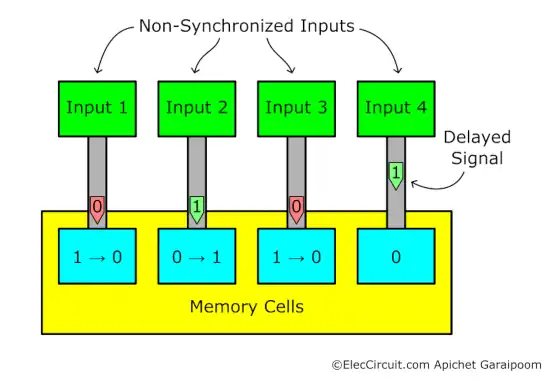
A great way to avoid this issue is to use a clock signal (often derived from a common clock generator or oscillator). This is to tell the signal source when to send the write signal and when the memory inputs should receive it.
Furthermore, we can also use the gated function to set a condition for the input to be enabled or disabled. For example, set it so that we cannot turn certain electronic appliances on or off until a certain condition has been met.
We will explore this idea further when we talk about the test circuit, but for now, let’s move on to understanding how the gated SR latch works logically.
Gated SR Latch From a Normal Latch
A gated SR latch (clocked SR flip-flop) has the same logical functionality as a normal SR latch. What is different is the addition of an enable (E) input. This E input functions as a sort of toggle switch for the S and R inputs, as we mentioned earlier.

The E input of a gated SR latch disables or enables the inputs of the SR latch, depending on the logic:
- When E = “0” → The Q output state will not change even if we apply S or R inputs.
- When E = “1” → The gated SR latch behaves like an SR latch.
We can construct the gated SR latch by adding a set of NAND or AND gates to the inputs of a normal SR latch. Let’s see the two ways to convert a normal SR latch into a gated one.
Gated SR AND-NOR Latch
For an active-high SR latch, such as the NOR gate SR latch, we can simply add two AND gates to the inputs. The SR latch and its inputs function remain unchanged. However, the S and R inputs now only work when the E (enable) input receives “1” logic.

The illustration above also shows the state-transition table. We can see that if the E input receives “0” logic, no matter the logic values of the S and R inputs, the Q output will hold its previous value (inputs disabled).
On the other hand, when E gets “1” logic, the gated SR latch functions as usual.
How the gated function works is very simple. As we should already know, an AND gate outputs “1” logic only when both of its inputs also receive “1” logic.
So, we can apply the SR latch input to the first AND gate input and then use the second input to create a gated condition. The SR latch input (AND gate output) only activates when the first input and the second input receive “1” logic.

The gated condition inputs for both AND gates usually combine into a single enable (E) input. This allows us to enable and disable both the S and R inputs together.
This method works with other active-high (non-inverted input) SR latches, such as the AND-OR SR latch. However, this will not work with active-low SR latches, like the NAND SR latch.
For an active-low (inverted input) SR latch, we need to use the NAND gate, which has the opposite function of the AND gate.
Gated SR NAND Latch
As for an active-low NAND SR latch, we can add another set of NAND gates to its input. The gate layout is the same as the AND version, except that we use a NAND gate instead of an AND gate.
Adding another set of NAND gates also changes the inverted input to a non-inverted input (active-high). So, instead of an active-low, a gated NAND SR latch is an active-high, similar to the previous one.
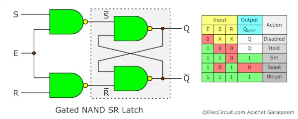
Because the inputs are not inverted, they no longer have a line above them. Plus, since this version of the gated SR latch is also an active-high latch, its state-transition table is the same as the previous one.
If the E input receives “0” logic, both S and R inputs are disabled. However, if the E input gets “1” logic, both inputs function normally as a non-inverted SR latch.
The NAND gating works in the same way as the AND one, but inverted. A NAND gate outputs “1” logic when at least one of its inputs gets “0” logic and outputs “0” logic when both inputs get “1.”
Therefore, if one or both of the NAND gate inputs receive “0” logic, the inverted SR latch gets “1,” which is its hold state. But if both inputs receive “1” logic, the inverted SR latch gets “0,” which is its active logic.
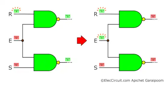
The gated condition using NAND only works with active-low (inverted input) latches. It also inverts the input of the latch (from active-low to active-high). This can be a positive, though, since we usually prefer active-high over active-low.
Simple Gated SR Latch Test Circuit Using LDR
Lastly for today, let’s make a simple circuit to test our understanding of the gated SR latch.
It is quite a simple circuit, consisting of switches to apply logic to the latch, an LED to see the output, and an LDR to set a condition for the latch inputs.

The LDR1 and R3 function as a voltage divider, and the voltage across LDR1 feeds directly into the enable input of the latch. With this LDR in place, one of the two scenarios described below will occur:
- If the LDR1 detects a high level of light, its resistance will increase, which means that the voltage across it will also increase. As a result, the enable input receives high voltage (E = “1” logic), and the latch operates as normal.
- If the LDR1 detects almost no light, its resistance will decrease, and the voltage across it will also decrease. Thus, the enable input receives low or no voltage (E = “0” logic), and the latch does not work.
To wrap things up, as we discussed earlier in the article, when the LDR1 detects light (E gets “1” logic), we can use switches S1 and S2 to control LED1. However, when LDR1 does not detect light (E gets “0” logic), switches S1 and S2 will not function, and LED1 holds its previous value.
Build the Test Circuit on the Breadboard

We also tested this circuit on a breadboard, as you can see in the image above. The circuit works as expected; nonetheless, it is still a simple test circuit only meant for learning.
If we want to use this circuit long-term or change the dependencies to something other than light (LDR), we should connect the enable input to a comparator rather than a simple voltage divider.
Lastly, we also have a few other articles related to the SR latch, which you can check out down below.
Learn About Two-Transistor SR Latch – How it Works Step-by-Step
Want to take this guide with you?
The full version includes deeper technical discussion, experimental insights, and clean PDF downloads with high-resolution diagrams — all ad-free.
✅ Read more: Learn How Gated SR Latch Works – With Example CircuitThank you for your support!
Hello. I’m Chayapol, but I could also go by Aot. I write and draw illustrations for ElecCircuit.com.
I usually cover articles related to digital electronics, logic, or basic principles or ideas on the site.